Key Takeaways
- Intel demonstrated a UCIe-S die-to-die interconnect on 22nm hitting 48 Gb/s/lane over standard organic substrate, beating a 3nm EMIB design with 3× higher data rate and 2.8× higher bandwidth density.
- This signals a strategic shift away from EMIB for Intel's own products toward UCIe over substrate.
Intel's UCIe-S Hits 48 Gb/s on 22nm, Beats 3nm EMIB
Intel is shifting its internal packaging strategy away from EMIB (Embedded Multi-die Interconnect Bridge) toward UCIe (Universal Chiplet Interconnect Express) over standard organic substrate — a move that could reshape its competitive position in advanced packaging. The company demonstrated the new interconnect at ISSCC, showing a UCIe-S die-to-die link on 22nm reaching 48 Gb/s/lane over standard organic substrate at a distance of up to 30 mm. That performance beats a 3nm EMIB design with 3× higher data rate and 2.8× higher bandwidth density.
What's Happening
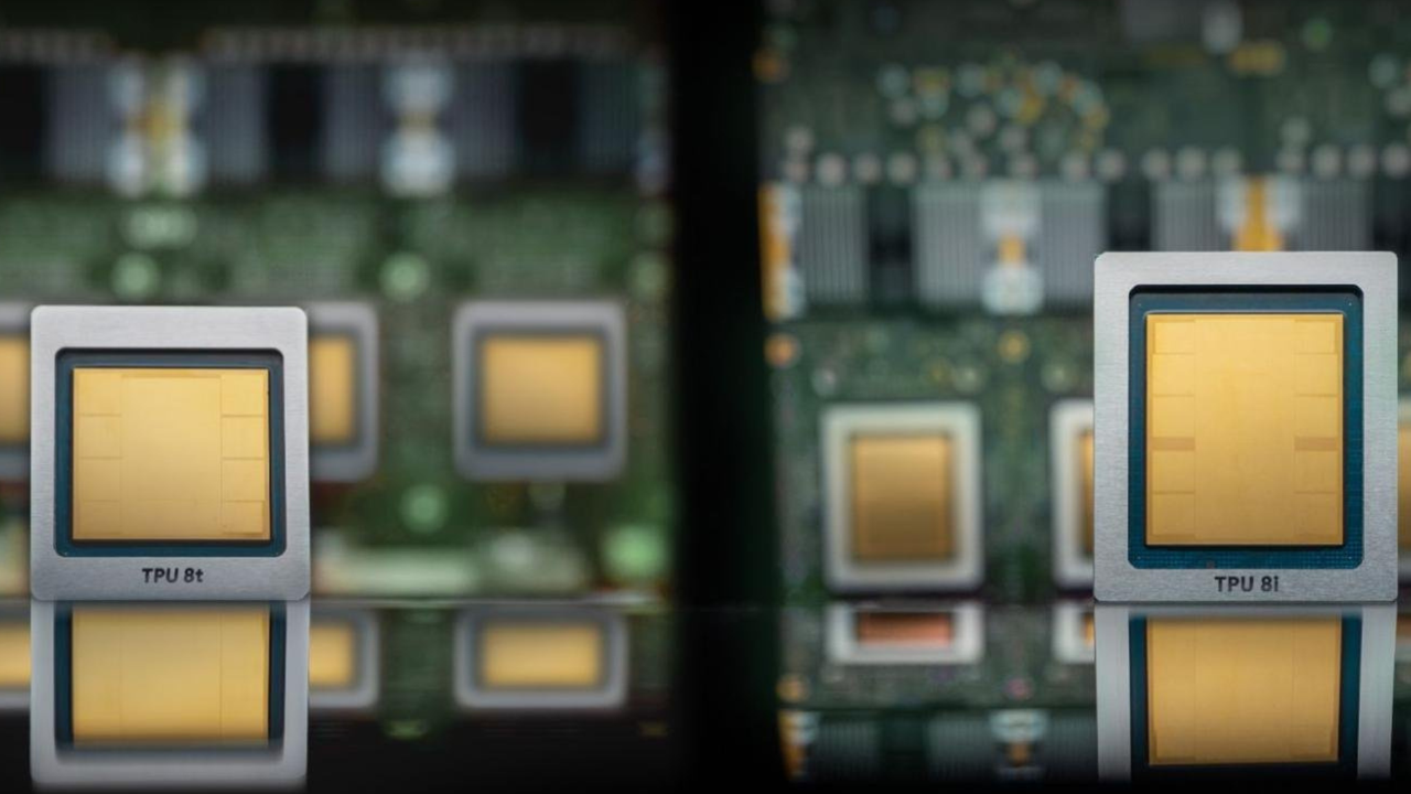
According to SemiAnalysis, Intel's Diamond Rapids processor will likely use UCIe over substrate for a long-reach die-to-die interconnect instead of EMIB. This is notable because Intel has been promoting EMIB externally — with Google's TPU being the marquee external customer — while moving away from it for its own products.
The key numbers from the ISSCC demo:
- Process node: 22nm (Intel's older node)
- Data rate: 48 Gb/s/lane
- Reach: Up to 30 mm over standard organic substrate
- Substrate stackup: 5-2-5 (vs 11-2-11 on EMIB)
- Comparison: 3× higher data rate, 2.8× higher bandwidth density vs a 3nm EMIB design
Why This Matters
The shift to UCIe over substrate has two major implications:
Substrate supply constraints: With substrate in short supply, Intel's "best" packaging technology — for everyone but Intel. The simpler 5-2-5 stackup reduces the number of substrate layers by more than half compared to EMIB's 11-2-11, easing manufacturing complexity and supply chain pressure.
Standardization advantage: UCIe is an open standard, backed by the UCIe Consortium (founded by Intel, AMD, ARM, and others in 2022). Moving to UCIe over substrate allows Intel to leverage an industry-standard interconnect rather than a proprietary bridge, potentially lowering costs and improving ecosystem compatibility.
How It Compares
Data rate 48 Gb/s/lane ~16 Gb/s/lane (estimated) Bandwidth density 2.8× higher Baseline Substrate stackup 5-2-5 11-2-11 Reach Up to 30 mm Limited by bridge Standard UCIe (open) ProprietaryWhat This Means in Practice
For chip designers and data center operators: Intel's move to UCIe over substrate means future Intel server processors (starting with Diamond Rapids) will use a simpler, more scalable interconnect that doesn't require the expensive embedded bridge technology. This could lead to lower packaging costs, faster time-to-market, and better supply chain resilience — but it also means Intel's most advanced packaging tech (EMIB) becomes a product for external customers like Google, not for Intel's own flagship chips.
The Bigger Picture
Intel's packaging strategy is undergoing a fundamental shift. The company is simultaneously:
- Selling EMIB externally: Google's TPU is the flagship customer
- Moving internally to UCIe over substrate: Diamond Rapids will use this
- Developing future packaging tech: Intel's roadmap includes Foveros (3D stacking) and hybrid bonding
This dual-track approach — selling premium packaging to competitors while using a simpler standard for its own products — reflects Intel's evolving role as a foundry and chip designer. It also highlights the growing importance of packaging as a differentiator in the AI and HPC era, where bandwidth and power efficiency between chiplets can make or break a system's performance.
gentic.news Analysis
Intel's UCIe-S demonstration is more than a technical benchmark — it's a strategic pivot. The company is effectively commoditizing its own advanced packaging for external customers while reserving a simpler, cheaper interconnect for its own processors. This mirrors Intel's broader foundry strategy: sell cutting-edge manufacturing to rivals while using proven, cost-effective nodes for its own products.
From a technical perspective, the 48 Gb/s/lane on 22nm is impressive because it shows that process node is not the only lever for performance. By optimizing the interconnect architecture and using standard organic substrate (which is cheaper and more available than the advanced substrates needed for EMIB), Intel achieves higher performance with older silicon. This is a pattern we've seen before: TSMC's CoWoS (Chip-on-Wafer-on-Substrate) packaging, which is critical for NVIDIA's AI GPUs, also uses mature nodes for the interposer.
However, there's a tension: Intel is simultaneously telling the market that its best packaging is EMIB (for external customers) while choosing UCIe over substrate for its own high-volume products. This could create confusion about Intel's packaging roadmap and raise questions about long-term investment in EMIB. If Intel's own chips don't use EMIB, why would external customers continue to invest in it?
Frequently Asked Questions
What is UCIe?
UCIe (Universal Chiplet Interconnect Express) is an open industry standard for die-to-die interconnects, enabling chiplets from different vendors to communicate. It was established in 2022 by Intel, AMD, ARM, and others to standardize chiplet integration.
How does UCIe-S compare to EMIB?
UCIe-S uses standard organic substrate for die-to-die communication, while EMIB uses an embedded silicon bridge. UCIe-S achieves higher data rates (48 Gb/s/lane) over longer distances (30 mm) with a simpler substrate stackup (5-2-5 vs 11-2-11), but EMIB offers higher density for very short distances.
Will Diamond Rapids use UCIe?
According to SemiAnalysis, yes. Intel's Diamond Rapids processor will likely use UCIe over substrate for long-reach die-to-die interconnects, moving away from EMIB for internal products.
Why is Intel moving away from EMIB for its own chips?
The primary reasons appear to be substrate supply constraints and cost. EMIB requires a complex 11-2-11 substrate stackup, while UCIe over substrate uses a simpler 5-2-5 stackup, reducing manufacturing complexity and improving supply chain resilience.