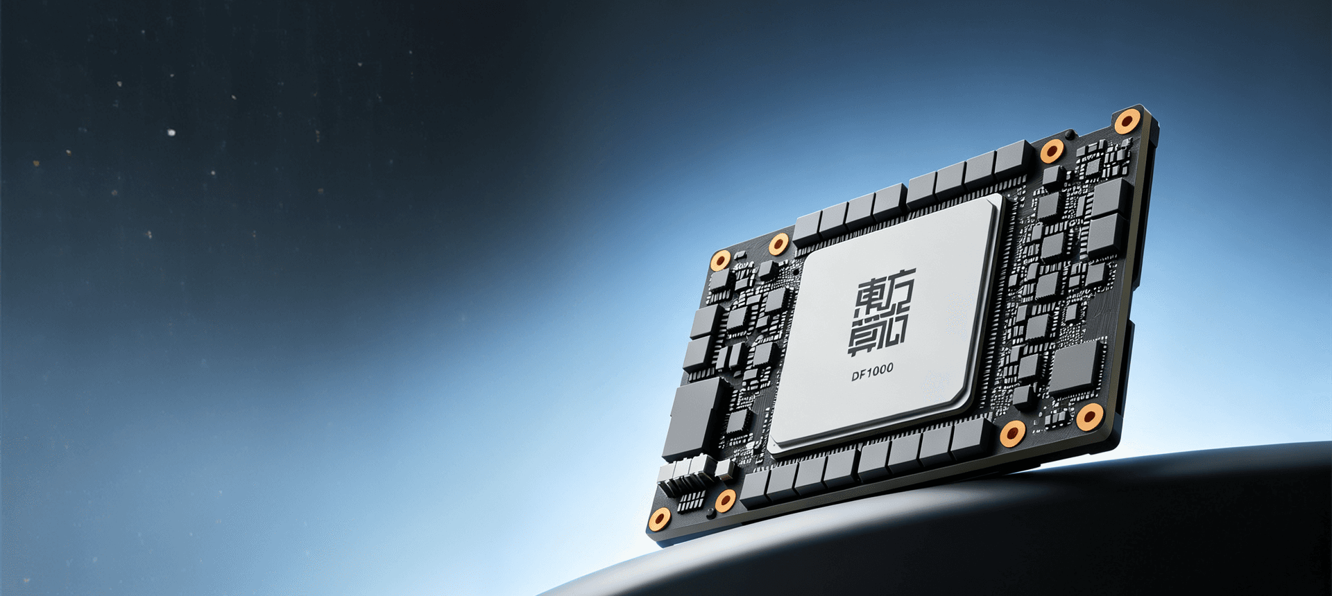
Dongfang Suanxin claims its 14nm AI chip delivers higher memory bandwidth than Nvidia's H200 GPU without using HBM. The Chinese firm's proprietary memory architecture aims to bypass US export controls that restrict HBM shipments to China.
Key facts
- 14nm process node used for the chip.
- Claims higher memory bandwidth than Nvidia H200 (4.8 TB/s).
- No HBM — proprietary memory architecture instead.
- US export controls restrict HBM shipments to China.
- No independent benchmarks or third-party verification yet.
Dongfang Suanxin, a Chinese semiconductor startup, unveiled an AI chip fabricated on a 14nm process that it claims achieves higher memory bandwidth than Nvidia's H200 GPU — without using High Bandwidth Memory (HBM) According to TrendForce. The chip reportedly uses a proprietary memory architecture that replaces the HBM stack with an alternative interconnect, though the company did not disclose specific technical details such as the exact bandwidth figure, compute performance (TFLOPS), or power consumption.
Strategic Context
The claim directly challenges US export controls that restrict HBM shipments to China. In 2026, the US Commerce Department tightened rules on HBM exports, requiring licenses for advanced memory stacks used in AI accelerators [as previously reported]. Dongfang Suanxin's approach — using a 14nm process (roughly equivalent to TSMC's 2014-era node) — mirrors other Chinese efforts to circumvent semiconductor sanctions by focusing on architectural innovation rather than process node scaling. The H200 uses HBM3e memory with a bandwidth of 4.8 TB/s, so Dongfang Suanxin's claim implies their chip exceeds that figure.
Skepticism Required
No independent benchmarks or third-party verification have been published yet. The company did not disclose the chip's compute performance or power consumption. The 14nm node, while cheaper and more accessible via Chinese foundries like SMIC, imposes significant density and power constraints compared to Nvidia's 4nm (N4) process used in the H200. A Chinese chip outperforming the H200 on memory bandwidth alone does not guarantee competitive AI training or inference throughput — memory bandwidth is one component of a system that also depends on compute density, interconnect fabric, and software stack maturity.
The announcement comes as Nvidia faces ongoing supply chain issues — its next-gen AI rack system was delayed to 2028 due to manufacturing snags [per recent history]. Meanwhile, the US has allowed some Chinese firms like ZTE to buy H200 chips [as reported on 2026-07-14], creating a fragmented export landscape.
What to watch
Watch for third-party benchmarks from Chinese research institutes or independent labs. If the chip ships to Chinese AI labs like Baidu or Alibaba, compare training throughput on models like Llama 3 70B against Nvidia H200 clusters. Also monitor US export policy — if the architecture proves viable, expect further restrictions on non-HBM memory technologies.
Source: news.google.com