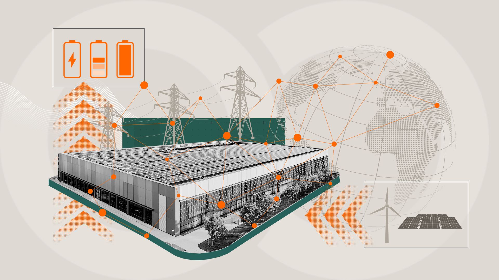
Nvidia has made a strategic $2 billion investment in Marvell Technology, a leading data infrastructure semiconductor company, to accelerate and expand their collaboration on NVLink Fusion technology. The investment represents a significant deepening of the partnership between the AI chip giant and the networking specialist, focusing on a critical bottleneck in AI infrastructure: high-speed chip-to-chip connectivity.
Key Takeaways
- Nvidia is investing $2 billion in Marvell Technology to deepen their partnership on NVLink Fusion, a chip-to-chip interconnect crucial for scaling AI training clusters.
- This strategic move aims to secure supply and accelerate development of high-bandwidth links between GPUs and custom AI accelerators.
What's New: A Strategic Investment in Interconnect Technology
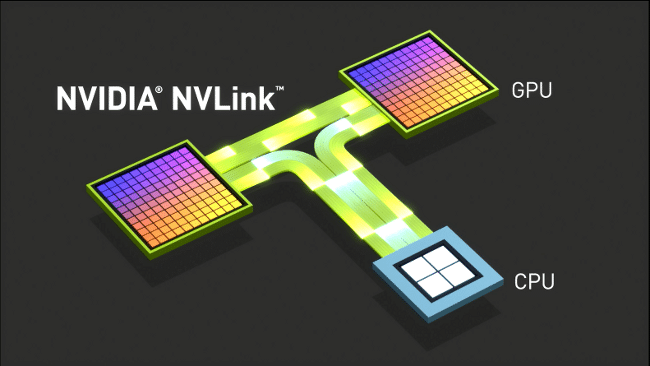
The $2 billion investment is not a simple financial play but a strategic move to secure and accelerate development of NVLink Fusion, a proprietary interconnect technology developed by Nvidia. NVLink Fusion represents an evolution beyond standard NVLink, designed to create seamless, high-bandwidth connections not just between Nvidia GPUs, but between GPUs and other processing elements like custom AI accelerators, CPUs, and memory.
This partnership aims to leverage Marvell's expertise in high-speed SerDes (Serializer/Deserializer) technology, optical interconnects, and custom silicon design to enhance NVLink Fusion's capabilities and manufacturing scale.
Technical Context: Why NVLink Fusion Matters
As AI models grow exponentially in size—with frontier models now exceeding trillions of parameters—the performance of training clusters is increasingly limited not by individual chip performance but by interconnect bandwidth between chips. Traditional networking protocols like InfiniBand or Ethernet introduce latency and bandwidth limitations that become critical bottlenecks at scale.
NVLink Fusion addresses this by creating a unified fabric that treats multiple chips as a single, massive computational unit. Key technical goals include:
- Extremely High Bandwidth: Targeting multiple terabits per second per link
- Low Latency: Sub-microsecond chip-to-chip communication
- Scalability: Supporting thousands of interconnected accelerators in a single logical system
- Heterogeneous Support: Connecting not just Nvidia GPUs but also custom AI accelerators from cloud providers and other chip designers
Marvell brings specific expertise in 112G and 224G SerDes technology, advanced packaging (including 2.5D and 3D integration), and optical interconnect solutions that are essential for implementing NVLink Fusion at scale.
Market Implications: Securing the AI Infrastructure Stack
This investment follows Nvidia's established pattern of vertical integration through strategic partnerships. Rather than attempting to build all interconnect technology in-house, Nvidia is leveraging Marvell's specialized expertise while maintaining control over the critical NVLink standard.
The move has several immediate implications:
Supply Chain Security: By investing directly in Marvell, Nvidia ensures priority access to advanced interconnect components that are becoming increasingly scarce as AI infrastructure demand surges.
Competitive Positioning: NVLink Fusion represents a key differentiator against competing AI accelerator ecosystems from AMD (with its Infinity Fabric) and various cloud providers developing custom chips. Making NVLink Fusion more capable and widely available strengthens Nvidia's ecosystem lock-in.
Heterogeneous Computing Enablement: As major cloud providers (AWS, Google, Microsoft) develop their own AI accelerators, they still need to connect these to Nvidia GPUs for certain workloads. An open(ish) NVLink Fusion standard could become the universal interconnect for heterogeneous AI clusters.
The Broader Trend: Interconnects as the New Battleground

This investment highlights a broader industry recognition: as Moore's Law slows, system performance gains increasingly come from advanced packaging and interconnects rather than transistor scaling. The ability to seamlessly connect multiple chips—whether through NVLink, UCIe (Universal Chiplet Interconnect Express), or proprietary alternatives—is becoming a critical competitive advantage.
Marvell has been positioning itself as a key enabler in this space, with previous partnerships across cloud providers and chip designers. Nvidia's investment validates this strategy and suggests Marvell's interconnect technology will play a central role in next-generation AI infrastructure.
What to Watch: Implementation Timeline and Competitive Response
The partnership's success will be measured by several concrete milestones:
- Product Availability: When will NVLink Fusion-enhanced systems reach the market?
- Performance Metrics: What bandwidth and latency improvements will be achieved over current NVLink 4.0 (900 GB/s)?
- Adoption Beyond Nvidia: Will other chip designers license NVLink Fusion for their accelerators?
- Competitive Developments: How will AMD, Intel, and the UCIe consortium respond to this strengthened Nvidia-Marvell alliance?
gentic.news Analysis
This investment represents a logical escalation in Nvidia's strategy to control the entire AI infrastructure stack. Following their previous investments in AI infrastructure companies and their acquisition of Mellanox in 2019 (which gave them InfiniBand expertise), this move targets the next bottleneck: chip-to-chip interconnects within the server node itself.
The timing is significant. As we've covered in our analysis of the Blackwell architecture rollout, Nvidia's next-generation platforms face increasing pressure from custom silicon alternatives from cloud hyperscalers. By making NVLink Fusion more capable and potentially more open, Nvidia is attempting to position its interconnect technology as the standard that even competing accelerators must adopt—a classic "embrace and extend" strategy.
This aligns with the broader trend we identified in our 2025 year-end review: the AI hardware ecosystem is bifurcating into general-purpose GPU providers and custom accelerator designers, with interconnect standards becoming the crucial interface between these worlds. Nvidia's investment suggests they intend to own that interface rather than cede it to open consortiums like UCIe.
Practically, AI engineers and infrastructure teams should expect NVLink Fusion to become a key specification in future server procurement decisions. The bandwidth and latency characteristics of this technology will directly impact training times for large models, making it as important as individual GPU performance for scale-out deployments.
Frequently Asked Questions
What is NVLink Fusion?
NVLink Fusion is Nvidia's next-generation chip-to-chip interconnect technology that extends beyond connecting just Nvidia GPUs. It aims to create a unified, high-bandwidth, low-latency fabric connecting GPUs, custom AI accelerators, CPUs, and memory in heterogeneous computing environments, treating them as a single computational system.
Why did Nvidia choose to invest in Marvell specifically?
Marvell possesses critical expertise in high-speed SerDes (Serializer/Deserializer) technology, advanced packaging solutions, and optical interconnects—all essential for implementing high-bandwidth chip-to-chip connections at scale. Marvell already has partnerships with major cloud providers and chip designers, making them a strategic partner for expanding NVLink Fusion's adoption beyond Nvidia's own ecosystem.
How does this affect competitors like AMD and Intel?
This investment strengthens Nvidia's position in the interconnect battleground, potentially making NVLink Fusion a de facto standard for high-performance AI clusters. Competitors will need to respond with enhanced versions of their own interconnect technologies (AMD's Infinity Fabric, Intel's CXL-based solutions) or consider adopting NVLink Fusion for compatibility with Nvidia-dominated ecosystems.
When will we see products using this enhanced NVLink Fusion technology?
While specific timelines haven't been announced, such strategic investments typically aim for product integration within 12-24 months. Given the rapid pace of AI hardware development, we might see early implementations in next-generation platforms following Nvidia's Blackwell architecture, potentially in 2027-2028 timeframe.