A significant bottleneck in the world's most advanced semiconductor manufacturing process is creating a potential shift in the AI hardware supply chain. According to industry analyst Rohan Paul, Taiwan Semiconductor Manufacturing Company (TSMC) has encountered a "hard capacity wall" at its 2-nanometer (2nm) production node. This constraint is reportedly opening a strategic window for Samsung Foundry to capture high-margin AI accelerator business from major technology firms.
What Happened
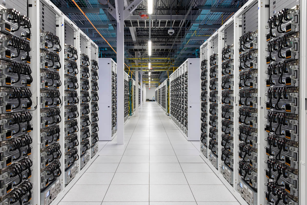
The core claim, based on industry analysis, is that TSMC—which currently manufactures the vast majority of the world's most advanced AI chips, including Nvidia's H100, H200, and B100 GPUs, as well as custom silicon for Google, Amazon, and Microsoft—is facing significant production capacity limitations at its next-generation 2nm process. This node is critical for the next wave of AI accelerators requiring higher performance and energy efficiency.
The "capacity wall" suggests that TSMC cannot scale 2nm production fast enough to meet the explosive demand forecast from AI chip designers. This creates a supply gap that competitors, primarily Samsung Foundry, could potentially fill.
Context: The AI Foundry Battle
TSMC has dominated the market for cutting-edge logic semiconductors for nearly a decade, enjoying a near-monopoly on manufacturing for companies like Apple, Nvidia, AMD, and numerous AI startups. Its 5nm and 4nm nodes power current-generation AI chips, and its 3nm process is ramping for future designs.
Samsung Foundry is TSMC's only credible competitor at the leading edge. It has been aggressively investing to close the technology and yield gap, offering its own 3nm Gate-All-Around (GAA) transistor technology and developing a 2nm node. Samsung has historically manufactured some of Nvidia's older GPU architectures and produces chips for its own devices and select clients, but has struggled to win high-volume, leading-edge AI business from TSMC's anchor customers.
A capacity shortage at TSMC's 2nm would force AI chip companies to pursue a multi-foundry strategy for risk mitigation. This is a scenario Samsung has been preparing for with significant capital expenditure and technology development.
Potential Implications
If accurate, this development could trigger several near-term effects:
Diversification Pressure on AI Chip Designers: Companies like Nvidia, AMD, and large hyperscalers designing custom AI ASICs (like Google's TPU, Amazon's Trainium, or Microsoft's Maia) may be compelled to qualify their next-generation designs at Samsung's 2nm process to ensure supply. This would break TSMC's de facto single-source hold on advanced AI silicon.
Accelerated Samsung Technology Roadmap: Samsung would likely receive increased investment and design partnership interest, potentially accelerating the maturity and yield of its 2nm GAA process.
Pricing and Contract Dynamics: Foundry pricing power could shift. TSMC's capacity constraints might allow it to maintain premium pricing, but the emergence of a viable second source could give large buyers more negotiation leverage in the long term.
Impact on AI Product Roadmaps: If 2nm chip supply is materially constrained industry-wide, it could delay the rollout or limit the volume of next-generation AI accelerators planned for 2026-2027, potentially affecting the pace of AI model scaling.
It is important to note that these are industry analyst observations. Neither TSMC nor Samsung has made an official statement confirming a specific 2nm capacity shortfall. Foundry capacity, yield, and timeline details are closely guarded competitive secrets.
gentic.news Analysis
This report aligns with a growing narrative of extreme tension in the advanced semiconductor supply chain, which we have covered extensively. In January 2026, we reported on the skyrocketing capital expenditure required for next-generation fabs, noting that TSMC's Arizona fab complex faced delays and rising costs. A capacity wall at 2nm is a logical extension of these macroeconomic and technical challenges—each new node requires more complex tools (especially High-NA EUV lithography), longer calibration times, and astronomically higher investment per wafer.
The entity relationship here is crucial. Samsung Foundry (📈) has been on a clear upward trend in our coverage, marked by its major $40 billion investment in Taylor, Texas in late 2025 and its successful qualification of 3nm GAA for select high-performance computing clients. A TSMC stumble at 2nm represents the precise opportunity Samsung's strategy has been designed to exploit. Furthermore, this connects directly to our December 2025 analysis of Nvidia's multi-foundry strategy, where CEO Jensen Huang explicitly discussed the need for a "resilient supply base." Nvidia is the single most important customer in this equation, and its next-generation "Rubin" GPU architecture, expected to use 2nm-class technology, would need guaranteed, high-volume supply.
This dynamic also intersects with the geopolitical landscape we've tracked. The concentration of leading-edge capacity in Taiwan has long been a concern for U.S. firms and policymakers. A stronger Samsung Foundry, with major capacity in the United States (Texas) and South Korea, offers a geographically diversified alternative, which could influence sourcing decisions beyond pure cost and performance metrics.
Ultimately, while TSMC's technology leadership is not in question, execution on capacity ramp is a different challenge. If this capacity constraint is real and prolonged, 2026-2027 could mark the most significant shift in leading-edge foundry market share in over a decade, with profound implications for who manufactures the brains of the AI era.
Frequently Asked Questions
What does "2nm" mean in chip manufacturing?
"2nm" refers to the 2-nanometer semiconductor manufacturing process node. It's a commercial label representing a new generation of transistor density and performance, not a literal measurement. Moving to a smaller node like 2nm allows chip designers to pack more transistors onto a chip, improving performance and energy efficiency—both critical for next-generation AI accelerators.
Why is TSMC so dominant in AI chip manufacturing?
TSMC has maintained a consistent lead in process technology, yield (percentage of working chips per wafer), and production scale for advanced nodes. Since AI chips from companies like Nvidia and AMD require the highest performance and are produced in massive volumes, they have relied almost exclusively on TSMC's cutting-edge 5nm, 4nm, and now 3nm processes. This has created a virtuous cycle where TSMC's revenue funds further R&D, cementing its lead.
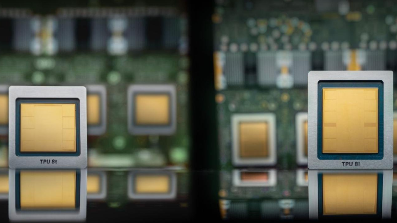
Has Samsung ever manufactured high-end AI chips before?
Yes, but not at the leading-edge volume of TSMC. Samsung manufactured Nvidia's RTX 30-series gaming GPUs during the previous generation and has produced various other components. However, for the flagship data center AI GPUs (like the H100) and the most advanced custom AI ASICs, TSMC has been the sole supplier. Samsung is aiming to change this with its 3nm GAA and future 2nm processes.
What could this mean for the cost and availability of future AI hardware?
In the short term, a tight supply of 2nm wafers could constrain the production volume of next-generation AI chips, potentially keeping prices high and limiting availability for cloud providers and AI labs. In the longer term, if Samsung becomes a viable second source, increased competition and supply could eventually help stabilize or reduce costs and improve availability, but this transition would take several years.