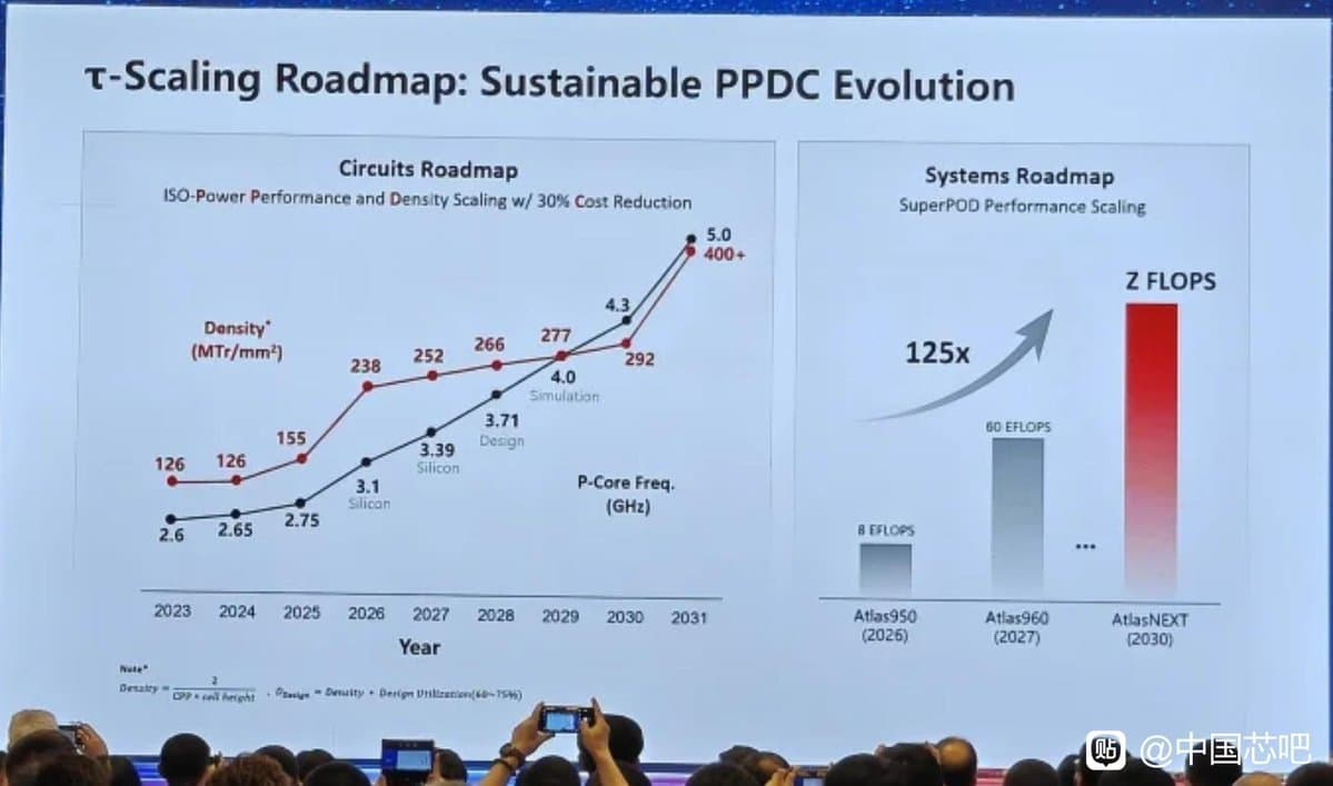
Huawei presented the Tau (τ) Scaling Law at IEEE ISCAS on May 18, 2026, replacing geometric transistor scaling with time-based optimization. The framework targets 1.4nm-equivalent transistor density by 2031 without EUV lithography, directly challenging US export control leverage.
Key facts
- Tau (τ) Scaling Law presented at IEEE ISCAS on May 18, 2026.
- 381 chips designed and mass-produced over six years.
- Targets 1.4nm equivalent density by 2031 without EUV.
- Kirin chips with LogicFolding architecture ship this fall.
- ASML EUV embargo remains in effect.
Huawei presented the Tau (τ) Scaling Law at IEEE ISCAS on May 18, 2026, replacing geometric transistor scaling with time-based optimization across devices, circuits, chips, and systems [According to @kimmonismus]. The framework abandons the nanometer race entirely, instead optimizing for temporal performance gains across the full stack.
How τ Scaling Works
Unlike traditional scaling laws that shrink transistor dimensions, τ Scaling optimizes time-based parameters — clock distribution, signal propagation delays, and circuit timing margins — across four abstraction levels: devices, circuits, chips, and systems. This allows Huawei to improve performance without shrinking feature sizes, bypassing the need for extreme ultraviolet (EUV) lithography, which remains under ASML embargo.
Huawei has already mass-produced 381 chips over six years using this approach, including Kirin processors with a new LogicFolding architecture shipping this fall [According to @kimmonismus]. The company's stated target is 1.4nm-equivalent transistor density by 2031, achieved entirely without EUV tools.
The Strategic Bet
The unique take: US export controls were designed to keep China two generations behind in semiconductor manufacturing. Huawei is making that metric irrelevant by redefining what 'generation' means. τ Scaling doesn't try to match TSMC's 2nm or Intel's 18A — it changes the race to one where density is a function of architectural optimization rather than lithographic precision.
If successful, this erodes the core leverage of US export controls: the assumption that cutting-edge lithography is necessary for cutting-edge performance. The sanctions were designed to force China into a nanometer gap they couldn't close. Huawei is building a parallel road.
What It Means for AI Workloads

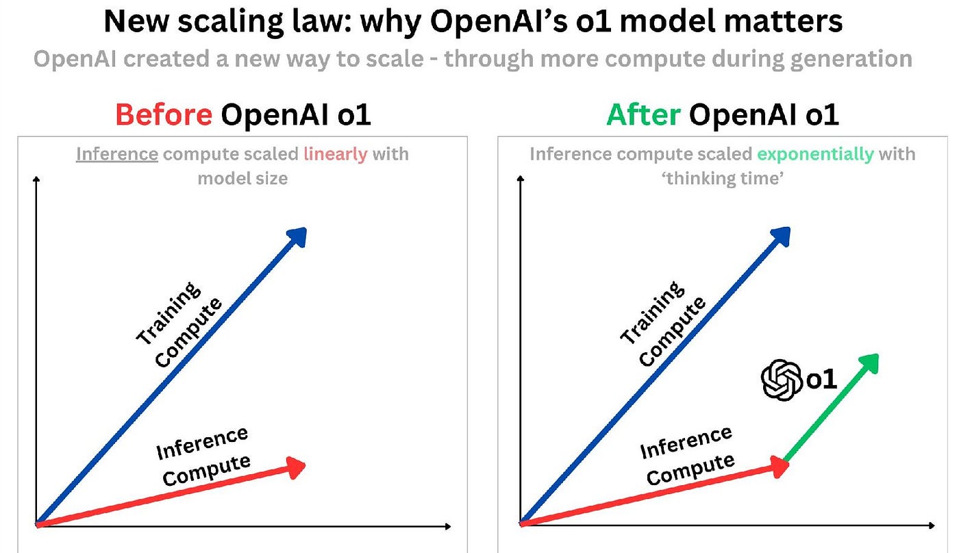
Huawei's Kirin chips already run AI workloads in shipping phones. τ Scaling's system-level optimization could yield particularly large gains for AI inference, where memory bandwidth and interconnect latency often dominate over raw transistor density. The framework's time-based approach directly targets these bottlenecks.
However, the company did not disclose specific benchmark results or performance comparisons against TSMC's 3nm or 2nm processes. Whether τ Scaling delivers on its 2031 promise remains unverified by independent analysis.
What to watch
Watch for independent benchmark results comparing Kirin LogicFolding chips against TSMC 3nm equivalents in Q4 2026. Also monitor whether other Chinese fabs adopt τ Scaling, and any US policy response if Huawei demonstrates competitive AI inference performance without EUV.
[Updated 27 May via scmp_tech]
In a parallel move that reinforces Huawei's strategy, China added AI chips to its official "secure and reliable" technology assessment list on Tuesday, creating a new category for "AI training and inference chips" [per SCMP]. The certification, issued by the China Information Technology Security Evaluation Centre, signals state backing for domestic alternatives to Western processors, potentially accelerating adoption of Huawei's Kirin LogicFolding chips in government and enterprise AI deployments.