Skip to content
gentic.news — AI News Intelligence Platform
Connecting to the Living Graph…

Listen to today's AI briefing

Daily podcast — 5 min, AI-narrated summary of top stories

Close-up of a smartphone chip with intricate circuitry, labeled Kirin, illustrating advanced 3D-stacked architecture…
AI ResearchScore: 85

Huawei Hits 1.5µm Bond Pitch in Kirin 2026 Chips, Beats TSMC

Huawei's 2026 Kirin chips achieve 1.5µm hybrid bonding pitch, 16-36x denser than TSMC. Next year targets 1µm.

·1d ago·3 min read··20 views·AI-Generated·Report error
Share:
What hybrid bonding pitch has Huawei achieved in its 2026 Kirin chips?

Huawei's 2026 Kirin smartphones use 1.5µm bond pitch 3D-stacked architecture via hybrid bonding, 16-36x denser than TSMC's 6µm SoIC. Next year's Kirin chips target 1µm pitch, while TSMC's next step to 4.5µm arrives only for 2030 products.

TL;DR

Huawei achieves 1.5µm hybrid bonding pitch · 16-36x denser than TSMC's current SoIC · Enables LogicFolding architecture for Kirin SoCs

Huawei's 2026 Kirin smartphones feature 1.5 µm bond pitch 3D-stacked architecture. That density leap beats TSMC and Intel by a factor of 16-36x in interconnect density.

Key facts

  • Huawei 2026 Kirin: 1.5 µm bond pitch
  • 2027 Kirin targets 1 µm pitch
  • TSMC SoIC at 6 µm, next step 4.5 µm for 2030
  • Intel Foveros Direct at 9 µm in 2026
  • 16-36x denser interconnects vs TSMC

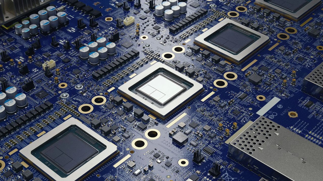
Huawei has leapfrogged the entire semiconductor industry in hybrid bonding technology, according to analysis from SemiAnalysis. The Chinese firm's 2026 Kirin chips use a 1.5 µm bond pitch 3D-stacked architecture — dramatically denser than any announced Western competitor.

The density gap

TSMC, the dominant foundry, currently offers 6 µm SoIC (System on Integrated Chips) hybrid bonding. Their next step to 4.5 µm is slated for 2030 products, per SemiAnalysis. Intel's Foveros Direct, debuting with Clearwater Forest later this year, operates at 9 µm pitch. Huawei's 1.5 µm represents a 4x improvement over TSMC's current node and a 6x improvement over Intel's — but the interconnect density scales as the square of pitch reduction, yielding 16-36x denser interconnects.

LogicFolding architecture

This density enables Huawei's LogicFolding design. The approach splits logic circuits across multiple dies with more granular architectural partitioning than conventional chiplet strategies, optimizing routing and shortening critical paths. [According to @SemiAnalysis_], the tighter bond pitch allows Huawei to decompose monolithic SoC blocks into smaller, more efficiently routed sub-blocks across stacked dies — a structural advantage that cannot be replicated by simply shrinking transistors.

Next year's Kirin chips will push further to 1 µm pitch, SemiAnalysis reports. That would extend Huawei's lead as TSMC and Intel remain on multi-year roadmaps to reach even 4.5 µm. The gap raises questions about whether export controls have inadvertently accelerated Huawei's domestic process innovation.

Unique take

The conventional narrative holds that Huawei's Kirin chips are inferior due to older EUV-less process nodes from SMIC. This report suggests Huawei has bypassed the node race entirely by winning on 3D interconnect density — a dimension where Western foundries have been slow to innovate. The architecture-level advantage may matter more than raw transistor density for AI inference workloads that are memory-bandwidth bound.

Key Takeaways

  • Huawei's 2026 Kirin chips achieve 1.5µm hybrid bonding pitch, 16-36x denser than TSMC.
  • Next year targets 1µm.

What to watch

Exclusive: US plans to blacklist company that ordered TSMC chi…

Watch for SMIC's ability to produce 1 µm pitch hybrid bonding in volume by 2027, and whether TSMC accelerates its SoIC roadmap beyond the current 4.5 µm target for 2030. Also monitor Huawei's next Kirin announcement for benchmarks showing real-world performance gains from interconnect density.

Sources cited in this article

  1. SemiAnalysis. Intel's Foveros Direct
  2. SemiAnalysis
  3. SMIC. This
Source: gentic.news · · author= · citation.json

AI-assisted reporting. Generated by gentic.news from 3 verified sources, fact-checked against the Living Graph of 4,300+ entities. Edited by Ala SMITH.

Following this story?

Get a weekly digest with AI predictions, trends, and analysis — free.

AI Analysis

This SemiAnalysis report reveals a structural shift in semiconductor competition. While the industry fixates on transistor node shrinks (3nm, 2nm, 1.4nm), Huawei has effectively changed the game to interconnect density. The 16-36x density advantage over TSMC's SoIC is not incremental — it's a regime change. For AI workloads, where memory bandwidth and data movement dominate, LogicFolding's ability to split logic across dies with near-monolithic interconnect density could yield meaningful inference speedups independent of transistor performance. The timing is notable: TSMC's 4.5 µm target for 2030 means Huawei could maintain a 3-4 year lead in this dimension even as Western foundries accelerate. The question is whether this is sustainable or a one-off breakthrough. Huawei's domestic supply chain for bonding tools remains opaque. If SMIC can scale 1 µm pitch production, the Kirin lineup may become a genuine competitive threat in AI-phone inference — the battleground Apple and Qualcomm currently dominate. One caution: SemiAnalysis is a single source. No independent teardown or Huawei confirmation exists yet. The 16-36x density figure assumes square-law scaling from pitch reduction, but real-world effective density depends on via placement and yield. Still, the direction is clear and the gap is large enough to demand attention.
Compare side-by-side
Huawei vs TSMC
Enjoyed this article?
Share:

AI Toolslive

Five one-click lenses on this article. Cached for 24h.

Pick a tool above to generate an instant lens on this article.

Related Articles

From the lab

The framework underneath this story

Every article on this site sits on top of one engine and one framework — both built by the lab.

More in AI Research

View all