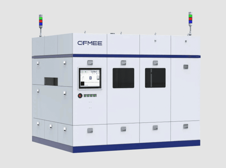
CFMEE's 510×515mm panel-level packaging (PLP) system passed validation, marking China's entry into advanced packaging for AI chips. The milestone challenges TSMC and Intel's dominance in chip packaging for high-performance AI accelerators.
Key facts
- CFMEE's 510×515mm PLP system passed validation.
- PLP can reduce costs per chip by up to 30%.
- Google booked Intel to package 3 million TPUs.
- TSMC's CoWoS capacity sold out through 2027.
- China faces US export controls on packaging equipment.
CFMEE's 510×515mm panel-level packaging (PLP) system passed validation, marking China's entry into advanced packaging for AI chips. The milestone, reported by TrendForce, positions CFMEE as a direct competitor to TSMC's InFO and Intel's EMIB packaging technologies.
Key Takeaways
- CFMEE validated a 510×515mm PLP system for AI chip packaging, challenging TSMC and Intel.
- The system targets HBM and AI accelerators, with potential 30% cost savings.
Why PLP Matters for AI
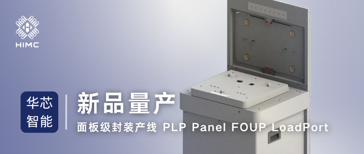
The 510×515mm panel size is larger than the standard 300mm wafer used in traditional fan-out wafer-level packaging. PLP can reduce costs per chip by up to 30% compared to wafer-level packaging, per industry estimates. For AI chips that require massive interconnects and high-bandwidth memory (HBM) integration, PLP offers better yield and lower defect rates due to the larger substrate area.
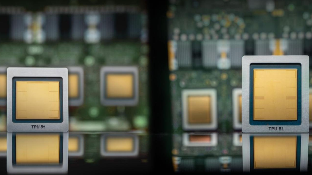
CFMEE's PLP system targets HBM and AI accelerator packaging, where TSMC's CoWoS and Intel's EMIB currently dominate. The validation comes as Google booked Intel to package 3 million TPUs by 2028, per a June 2025 report. If CFMEE can scale production, it could offer an alternative supply chain for Chinese AI chip designers like Huawei and Biren, who face US export controls on advanced packaging.
Geopolitical Context
The PLP validation is part of China's broader push to self-sufficiency in semiconductor manufacturing. The US has restricted exports of advanced packaging equipment to China, including tools from Applied Materials and ASM International. CFMEE's system uses domestic supply chain, according to TrendForce, though the company did not disclose specific equipment partners or production timelines.
China's entry into PLP mirrors its strategy in other chipmaking domains: start with mature nodes and scale. The 510×515mm panel is not the largest in the industry — Samsung and JCET have demonstrated 600×600mm panels — but it represents a credible first step for a Chinese supplier.
Competitive Landscape
TSMC and Intel have invested billions in advanced packaging. TSMC's CoWoS capacity is sold out through 2027, with prices exceeding $10,000 per wafer for HBM integration. Intel's EMIB-T packaging for Google's TPUs uses a different approach, interconnecting multiple chiplets on an interposer. CFMEE's PLP competes directly on cost and substrate size, but lacks the ecosystem and reliability track record of incumbents.
The validation is a proof-of-concept, not a production ramp. CFMEE did not disclose yield rates, throughput, or customer commitments. Without volume, the PLP system remains a lab achievement.
What to watch
Watch for CFMEE's first commercial customer announcement and yield data. If a Chinese AI chip designer like Huawei or Biren publicly adopts the PLP system, it signals production readiness. Also monitor US export controls on packaging equipment for potential tightening.
Source: news.google.com