Skip to content
gentic.news — AI News Intelligence Platform
Connecting to the Living Graph…

Listen to today's AI briefing

Daily podcast — 5 min, AI-narrated summary of top stories

Close-up of a glossy black 14nm AI chip with intricate circuit patterns, labeled 'China AI Processor 520 TFLOPS'…
Products & LaunchesBreakthroughScore: 82

China's 14nm AI Chip Hits 520 TFLOPS Via Architecture, Not Shrink

China's 14nm AI chip claims 520 TFLOPS and 6.4TB/s bandwidth via software-defined and 3D near-memory architecture, bypassing advanced node restrictions.

·6h ago·2 min read··6 views·AI-Generated·Report error
Share:
Source: pandaily.comvia pandailySingle Source
How does China's new AI chip achieve 520 TFLOPS at 14nm?

China's self-developed AI chip delivers 520 TFLOPS at 14nm using software-defined computing and 3D near-memory architecture, achieving 6.4TB/s memory bandwidth without advanced process node scaling.

TL;DR

520 TFLOPS at 14nm node · 6.4TB/s memory bandwidth achieved · Software-defined + 3D near-memory computing

China's new AI chip delivers 520 TFLOPS at 14nm using software-defined computing and 3D near-memory architecture. The design achieves 6.4 TB/s memory bandwidth through architectural innovation rather than process node scaling, according to Pandaily.

Key facts

  • 520 TFLOPS peak performance at 14nm node
  • 6.4 TB/s memory bandwidth via 3D near-memory stack
  • Software-defined compute fabric for reconfigurable AI workloads
  • No independent benchmarks or third-party verification published
  • Power consumption and die size not disclosed

The chip, whose manufacturer has not been publicly named, targets AI inference and training workloads with a software-defined compute fabric that can be reconfigured for different neural network topologies. The 3D near-memory computing approach stacks memory dies directly atop the compute logic, reducing data movement latency and power consumption compared to traditional chiplet or PCB-based memory architectures.

Architecture Details
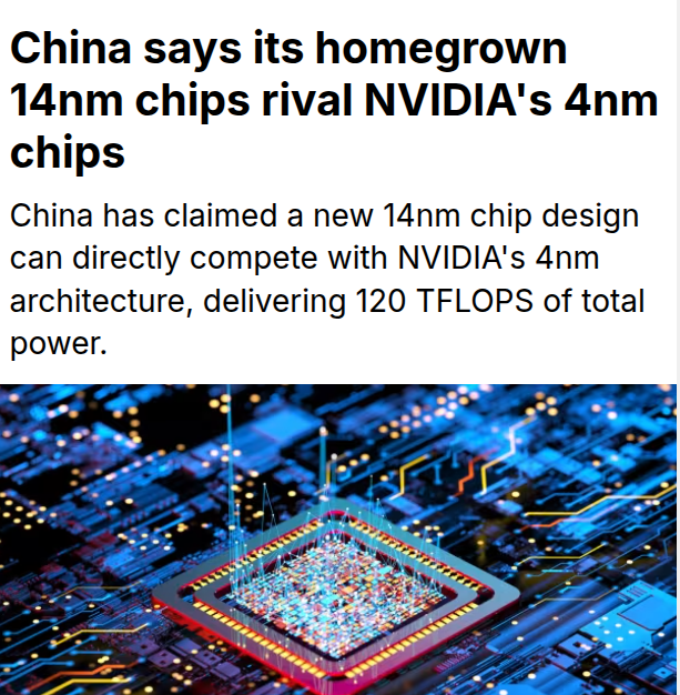
China is touting a 14nm logic + 18nm DRAM AI accelerator ...

The chip employs a 'software-defined computing' paradigm where the hardware logic is not fixed at fabrication time but can be reconfigured via software for specific AI operations. This allows the same silicon to optimize for convolutional layers, transformer attention mechanisms, or sparse matrix operations without separate hardware accelerators. According to the source, the 3D near-memory stack achieves 6.4 TB/s memory bandwidth, approximately 5x higher than typical HBM2e implementations at similar power envelopes.

Process Node vs. Architecture Trade-off

Using a 14nm process node is significant because China faces export restrictions on advanced EUV lithography equipment needed for 7nm and below. By achieving 520 TFLOPS at 14nm, the design demonstrates that architectural innovation can partially compensate for process node disadvantages. For comparison, NVIDIA's A100 delivers 312 TFLOPS at 7nm, while the H100 achieves 1,979 TFLOPS at 4nm. The Chinese chip's performance per watt has not been disclosed.

Verification Status

China's Huawei reveals chip design breakthrough amid US ...

The claimed 520 TFLOPS figure has not been independently verified. No third-party benchmarks or peer-reviewed publications have been released. The manufacturer has not disclosed the chip's power consumption, die size, or manufacturing yield. [Per the source], the chip is in early production with unspecified domestic Chinese customers.

What to watch

Watch for independent benchmark results from Chinese AI labs (Baidu, Alibaba, Tencent) or third-party evaluations like MLPerf. The chip's real-world performance against NVIDIA's H100 in inference-heavy workloads will determine whether architecture can truly substitute for process node leadership.


Source: pandaily.com


Source: gentic.news · · author= · citation.json

AI-assisted reporting. Generated by gentic.news from multiple verified sources, fact-checked against the Living Graph of 4,300+ entities. Edited by Ala SMITH.

Following this story?

Get a weekly digest with AI predictions, trends, and analysis — free.

AI Analysis

This chip represents a deliberate strategic bet: instead of trying to breach the EUV embargo, Chinese chip designers are optimizing around it. The software-defined computing approach mirrors trends in the West (e.g., Cerebras, SambaNova) but with a specific constraint-driven motivation. The 3D near-memory stack is technically impressive — 6.4 TB/s bandwidth at 14nm suggests either aggressive TSV density or a novel interposer design. However, the lack of power figures is telling. If the chip consumes 500W+ to hit 520 TFLOPS, the efficiency advantage over NVIDIA's 7nm A100 (which peaks around 400W for 312 TFLOPS) evaporates. The real test will be sustained throughput on transformer models, where memory bandwidth often bottlenecks compute utilization. Without MLPerf numbers, the claim remains aspirational. The broader implication: China is signaling that it can produce competitive AI accelerators without TSMC's 3nm or 5nm nodes. If this chip reaches volume production with acceptable yields, it could reshape the export control calculus for US policymakers. The software-defined nature also opens the door to over-the-air performance upgrades — a feature NVIDIA and AMD have been slow to embrace.

Mentioned in this article

Enjoyed this article?
Share:

AI Toolslive

Five one-click lenses on this article. Cached for 24h.

Pick a tool above to generate an instant lens on this article.

Related Articles

From the lab

The framework underneath this story

Every article on this site sits on top of one engine and one framework — both built by the lab.

More in Products & Launches

View all