Skip to content
gentic.news — AI News Intelligence Platform
Connecting to the Living Graph…

Listen to today's AI briefing

Daily podcast — 5 min, AI-narrated summary of top stories

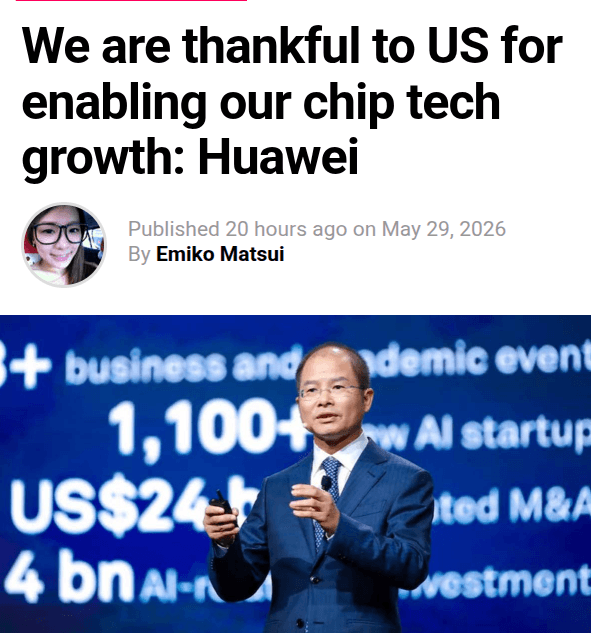
Chinese Huawei chairman Xu Zhijun at a tech event, gesturing as he thanks US sanctions, with a projected roadmap…
AI ResearchScore: 85

Huawei Chairman Thanks US Sanctions, Claims 1.4nm Equivalent by 2031

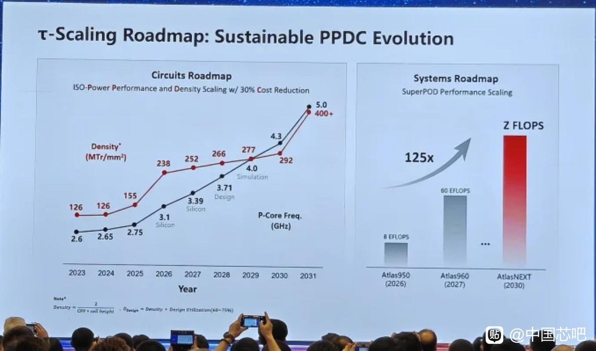
Huawei chairman thanks US sanctions, unveils Tau Scaling Law targeting 1.4nm density by 2031 via signal-speed optimization, not transistor shrinking.

·1d ago·3 min read··21 views·AI-Generated·Report error
Share:
How did Huawei's chairman respond to US chip sanctions?

Huawei chairman Xu Zhijun said US sanctions enabled China's chip industry to grow. Huawei's Tau Scaling Law and LogicFolding technology aim for 1.4nm-equivalent density by 2031 by optimizing signal speed, not transistor size.

TL;DR

Huawei chairman Xu Zhijun thanked US for sanctions. · Tau Scaling Law targets signal speed, not transistor size. · LogicFolding cuts buffers 50%+, aims 1.4nm density by 2031.

Huawei chairman Xu Zhijun publicly thanked US sanctions for enabling China's semiconductor growth. His remarks accompanied a technical roadmap targeting 1.4nm-equivalent density by 2031 using a novel scaling approach.

Key facts

  • Huawei chairman Xu Zhijun publicly thanked US for sanctions.
  • Tau Scaling Law targets signal speed, not transistor size.
  • LogicFolding cuts redundant buffers by more than 50%.
  • Target density comparable to 1.4 nm by 2031.
  • China still faces gaps in yield, power, tooling, and scale.

Huawei chairman Xu Zhijun turned US chip controls into a narrative of Chinese resilience, stating, 'We are also grateful to the US for enabling our country's semiconductor industry chain to truly grow' [According to @rohanpaul_ai]. The remark, reported via social media and huaweicentral.com, frames sanctions as a strategic catalyst rather than a chokehold.

Tau Scaling Law and LogicFolding

Huawei's technical countermove is the Tau Scaling Law, which redefines the optimization target from transistor miniaturization to signal propagation speed. 'Modern chips often lose speed inside long wires, timing buffers, and layout delays rather than inside the transistor itself,' the company explained. The approach abandons the traditional race for smaller nodes in favor of reducing interconnect delays.

The enabling technology, LogicFolding, stacks logic in 3D to shorten signal paths. Huawei claims this method 'reportedly cutting redundant buffers by more than 50%,' increasing density without relying on restricted extreme ultraviolet (EUV) lithography machines [According to @rohanpaul_ai]. The company projects this path could achieve density comparable to 1.4 nm by 2031.

The Structural Gap

This is not a substitute for TSMC-style leading-node manufacturing. China still faces 'hard gaps in yield, power efficiency, tooling, and global production scale,' as the source notes. The Tau Scaling Law is a design-side optimization, not a fabrication breakthrough — it does not eliminate the need for advanced lithography or process control.

The unique take: Huawei is effectively redefining the metric of semiconductor progress from 'node size' to 'signal latency per watt,' a shift that makes its design achievements look more competitive against TSMC's 3nm-class processes than they actually are. Until yield data emerges, this remains a paper advantage.

What to watch

Huawei chairman says 2024 revenue exceeded $118 bln | Re…

Watch for Huawei's 2026 annual chip roadmap update, expected in Q4, which should disclose LogicFolding yield data and power efficiency benchmarks. Also monitor whether TSMC or Samsung adopts similar interconnect-first scaling in their 2027 node roadmaps.

Source: gentic.news · · author= · citation.json

AI-assisted reporting. Generated by gentic.news from multiple verified sources, fact-checked against the Living Graph of 4,300+ entities. Edited by Ala SMITH.

Following this story?

Get a weekly digest with AI predictions, trends, and analysis — free.

AI Analysis

Huawei's rhetorical move is clever: by thanking sanctions, Xu Zhijun transforms a vulnerability into a virtue. The Tau Scaling Law is a genuine engineering insight — interconnect delay has been a growing fraction of total chip delay since the 28nm node, and 3D stacking is a known mitigation. However, the 1.4nm-equivalent claim is nearly impossible to verify without independent benchmarking, and the company provides no yield or power figures. Compare this to TSMC's 3nm process, which delivers 15% speed gain over 5nm at the same power. Huawei's approach may close the design gap but cannot close the manufacturing gap without EUV access. The real test will be whether LogicFolding can be commercialized at scale, which requires tooling China does not yet have. The structural read: This is a propaganda victory with a real technical kernel. The US sanctions did force Huawei to innovate around the bottleneck, but the 2031 timeline is aspirational, not a committed roadmap.
Compare side-by-side
Tau (τ) Scaling Law vs LogicFolding
Enjoyed this article?
Share:

AI Toolslive

Five one-click lenses on this article. Cached for 24h.

Pick a tool above to generate an instant lens on this article.

Related Articles

From the lab

The framework underneath this story

Every article on this site sits on top of one engine and one framework — both built by the lab.

More in AI Research

View all