POSTECH researchers achieved stable 10+ layer chip stacking with 4× the density of 12-Hi HBM. The breakthrough targets the memory bandwidth bottleneck constraining AI inference accelerators.
Key facts
- POSTECH achieved 10+ layer chip stacking.
- 4× density compared to 12-Hi HBM.
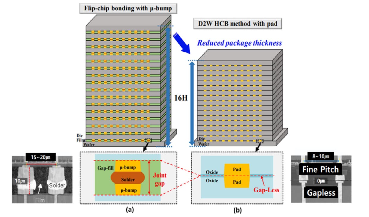
- Uses hybrid bonding (Cu-Cu + oxide fusion).
- Targets AI inference memory bandwidth bottleneck.
- No commercialization timeline announced.
POSTECH (Pohang University of Science and Technology) announced a chip-stacking technology that achieves stable operation at 10+ layers, delivering 4× the interconnect density of current 12-Hi HBM (High Bandwidth Memory) stacks. The result was reported by TrendForce on July 10, 2026.
Why It Matters for AI Inference
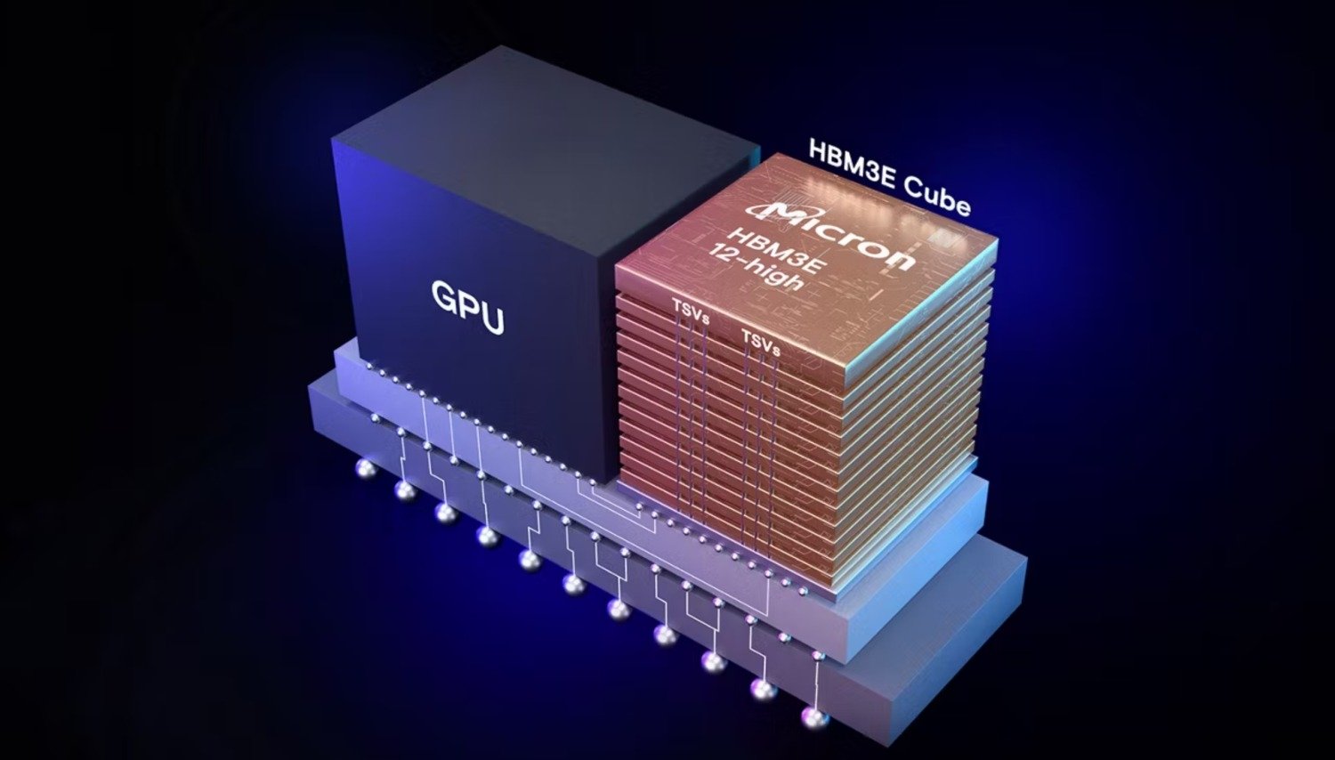
The 10+ layer stacking targets the memory bandwidth bottleneck in AI inference workloads. Current HBM3E stacks peak at 12 layers (12-Hi) with bandwidth around 1.2 TB/s per stack. POSTECH's approach uses a hybrid bonding technique—combining direct copper-to-copper bonding with oxide-oxide fusion—to reduce layer thickness and improve thermal dissipation. The result is a denser vertical interconnect that could enable higher bandwidth per stack without increasing physical footprint.
Density vs. Commercial Reality
While 4× density over 12-Hi HBM is impressive on paper, the technology remains at the university research stage with no announced commercialization timeline. HBM manufacturers (Samsung, SK hynix, Micron) have already roadmaped 16-Hi and 20-Hi stacks for 2027–2028, though with diminishing returns on density due to thermal and yield challenges. POSTECH's hybrid bonding could leapfrog those roadmaps if scaled, but the gap between lab demo and volume production is wide.
Comparison to Prior Art
The result echoes earlier work by imec and TSMC on hybrid bonding for 3D NAND and logic-on-logic stacking. POSTECH's contribution is specific to DRAM-like memory stacking, where layer count above 8 has historically caused thermal runaway and signal integrity degradation. The team did not disclose the exact layer count beyond "10+" or the specific test chip yields.
What to watch
Watch for POSTECH to publish a peer-reviewed paper with exact layer count, yield data, and thermal measurements. Also monitor whether Samsung or SK hynix license the hybrid bonding technique for their 2028 HBM4E roadmaps.
Source: news.google.com