While AI headlines focus on model architectures and algorithmic breakthroughs, the physical foundation of the intelligence explosion is undergoing a historic build-out. The world's leading semiconductor foundry, Taiwan Semiconductor Manufacturing Company (TSMC), is executing the largest manufacturing expansion in its history to meet the voracious compute demands of advanced AI systems.
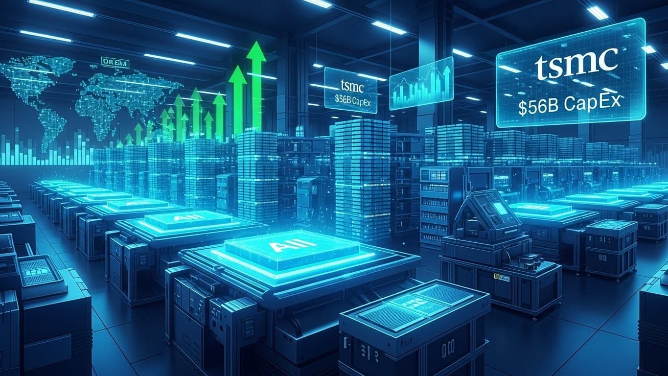
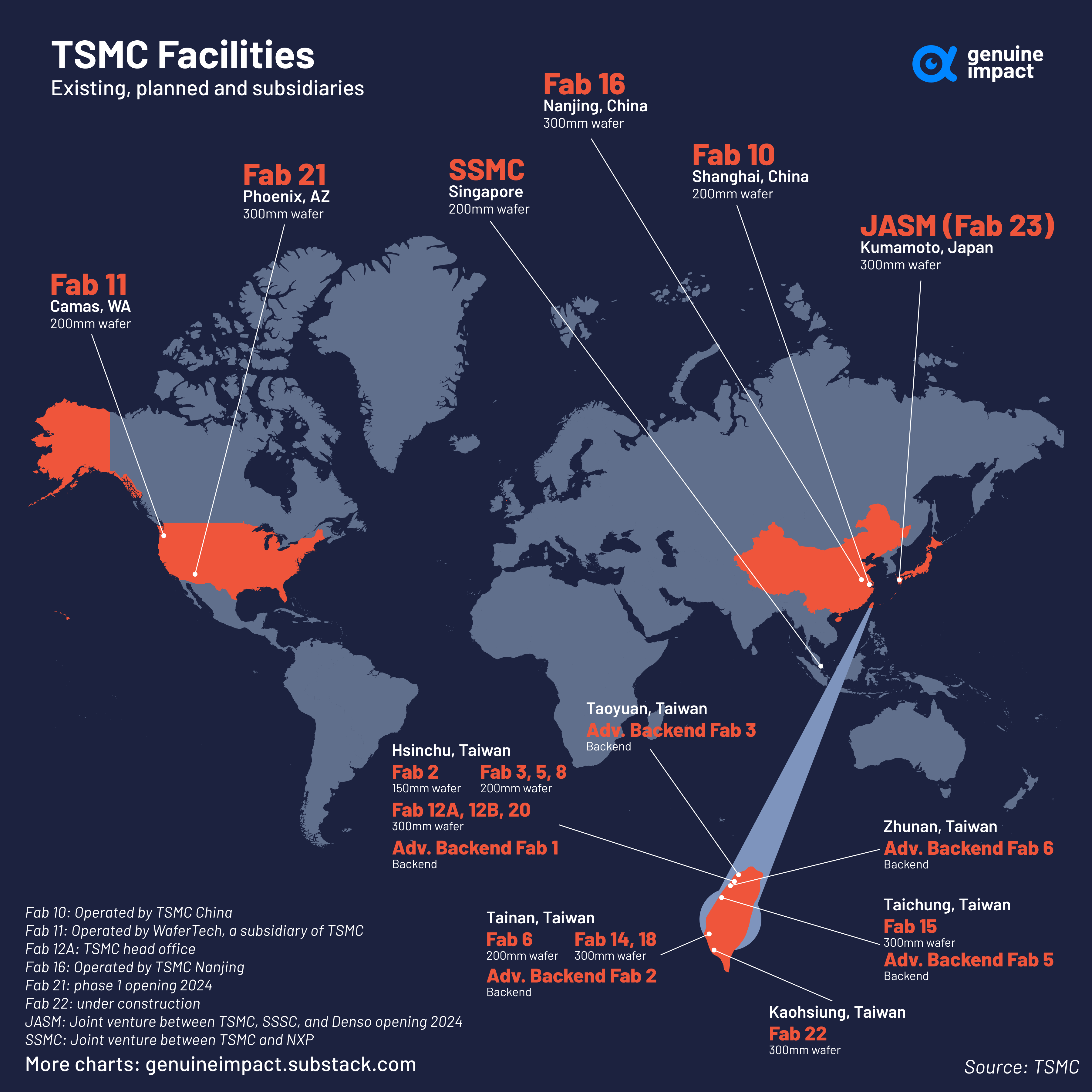
According to analysis shared by industry observer @kimmonismus, TSMC is currently building up to 10 fabs simultaneously in Taiwan while expanding to 12 fabs in Arizona, USA. This construction frenzy is backed by a staggering capital expenditure (CapEx) budget of $52–56 billion for 2026 alone, representing a 30% year-over-year increase.
Key Takeaways
- TSMC is constructing up to 22 advanced semiconductor fabs simultaneously, backed by a $52–56 billion capital expenditure plan for 2026.
- This unprecedented manufacturing scale is critical for producing the 2nm-and-below chips required by next-generation AI models.
The Scale of the Build-Out
This isn't a marginal increase in production capacity. It's a strategic scaling at the most advanced and expensive process nodes.
- Global Footprint: 22 new fabrication facilities under concurrent construction.
- Financial Commitment: $52–56 billion planned CapEx for 2026. For context, TSMC's total CapEx from 2019 to 2023 was approximately $172 billion. The 2026 figure represents nearly one-third of that five-year total in a single year.
- U.S. Investment: The Arizona complex is part of a total U.S. investment reaching $165 billion, noted as the largest foreign direct investment in American history.
Why This Matters for AI
The core thesis is that AI progress is no longer bottlenecked solely by algorithms or chip design, but by the ability to manufacture enough of the most advanced chips. Each new generation of large language models (LLMs) and multimodal AI requires exponentially more transistors and specialized compute.
TSMC's expansion is specifically targeted at the 2nm and below process frontier. Moving to these advanced nodes is astronomically expensive—the cost per wafer increases dramatically—but it delivers the transistor density and power efficiency that AI infrastructure fundamentally demands. Without this manufacturing scale, the industry would hit a physical compute wall, regardless of software innovations.
As @kimmonismus notes, this is about "scaling compute density at the frontier." It's a parallel race to the one happening in AI labs: a race to build the factories that will build the brains.
gentic.news Analysis

This data point is a critical piece of hardware reality that contextualizes the entire AI boom. It follows a pattern we've tracked closely: the convergence of unprecedented capital investment, geopolitical industrial policy, and pure technological necessity.
This TSMC expansion directly supports the roadmaps of its primary AI clients. NVIDIA, which designs the dominant H100, H200, and Blackwell GPUs, relies entirely on TSMC's advanced packaging (CoWoS) and 4nm/3nm processes. AMD's MI300 series and upcoming chips are also fabbed at TSMC. Even companies designing their own AI accelerators, like Amazon (Trainium/Inferentia), Google (TPU), and Microsoft (Maia), are dependent on TSMC's manufacturing leadership. This build-out mitigates a critical supply chain risk for all of them.
This aligns with our previous coverage on the U.S. CHIPS Act and the global subsidy war for semiconductor sovereignty. The $165 billion U.S. investment figure underscores that AI chip production is now a top-tier geopolitical priority, not just a corporate strategy. The scale of this investment—dwarfing most other industrial projects—validates the long-term bet that AI compute demand will continue its exponential curve for the foreseeable future.
For AI practitioners, the implication is clear: the hardware runway for model scaling is being extended. Concerns about a near-term physical limit to training compute are being addressed by the largest industrial mobilization in tech history. The bottleneck is shifting from transistor supply back to algorithmic efficiency, energy availability, and data.
Frequently Asked Questions
How many new fabs is TSMC building?
TSMC is currently constructing up to 22 new semiconductor fabrication plants (fabs) simultaneously. This includes up to 10 fabs in Taiwan and 12 fabs as part of its expanding campus in Arizona, USA.
Why is TSMC spending so much on new fabs?
The primary driver is the explosive demand for advanced AI chips. Training and running state-of-the-art large language models and multimodal AI requires massive amounts of compute, which in turn requires the most advanced semiconductors (2nm process and below). TSMC's expansion is a direct response to orders from AI chip designers like NVIDIA, AMD, and major cloud providers building custom AI silicon.
What is the significance of moving to 2nm and below processes?
Smaller process nodes (measured in nanometers) allow for more transistors to be packed onto a single chip. This increases computational power and energy efficiency dramatically. For AI workloads, this translates to faster training times, lower inference latency, and the ability to build larger, more capable models. Each step to a smaller node is exponentially more expensive but necessary for AI progress.
Is this just about making more chips, or better chips?
It's about both volume and capability. The new fabs are being built to produce chips at the most advanced "frontier" nodes (2nm and below). This scales the production of the highest-performance, most power-efficient silicon that AI systems require. It's not just increasing output of existing designs; it's enabling the production of next-generation designs that would be impossible on older manufacturing processes.