Skip to content
gentic.news — AI News Intelligence Platform
Connecting to the Living Graph…

Listen to today's AI briefing

Daily podcast — 5 min, AI-narrated summary of top stories

A scientist in a cleanroom lab adjusts a microscope above a silicon wafer; the screen displays nanoscale circuit…
AI ResearchBreakthroughScore: 90

Chinese Team Claims Carbon Nanotube CFET Breakthrough; Challenges TSMC at 2nm

Chinese team claims 3x carbon nanotube CFET gain over silicon at 2nm, bypassing EUV. No peer review; skepticism warranted.

·1d ago·3 min read··16 views·AI-Generated·Report error
Share:
Source: news.google.comvia trendforce_gnMulti-Source
What did a Chinese team achieve with carbon nanotube CFET architecture?

A Chinese research team reported a breakthrough in carbon nanotube complementary FET (CFET) architecture, claiming a 3x performance improvement over silicon at 2nm node, potentially bypassing EUV lithography constraints.

TL;DR

Chinese team achieves carbon nanotube CFET. · Claims 3x performance gain vs. silicon. · Could bypass EUV lithography bottleneck.

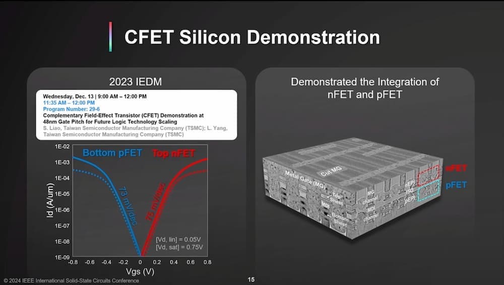
A Chinese research team reported a breakthrough in carbon nanotube complementary FET (CFET) architecture. The team claims a 3x performance improvement over silicon at equivalent 2nm node dimensions, potentially bypassing EUV lithography constraints.

Key facts

  • 3x claimed performance gain over silicon at 2nm.
  • Carbon nanotube CFET bypasses EUV lithography.
  • China's domestic AI chip budget rose to 46%.
  • No peer-reviewed paper or benchmark data published.
  • DeepSeek, Zhipu exploring custom silicon alternatives.

A Chinese research team reported a breakthrough in carbon nanotube complementary FET (CFET) architecture, claiming a 3x performance improvement over silicon at equivalent 2nm node dimensions. The carbon nanotube CFET design could bypass EUV lithography constraints entirely, a critical advantage as TSMC and Samsung struggle with yield at 2nm. According to TrendForce

The breakthrough arrives as China's domestic AI chip budget share reportedly rose from 30% to 46%, per TrendForce, driven by DeepSeek and Zhipu exploring custom silicon. The carbon nanotube CFET approach promises denser, lower-power transistors without requiring extreme ultraviolet (EUV) lithography — a technology China cannot access due to US export controls. The team did not disclose fabrication yield, energy-delay product, or specific benchmark results.

No peer-reviewed paper or benchmark data has been published yet. The claim should be treated with skepticism until independent verification emerges. Previous Chinese carbon nanotube transistor claims in 2024 proved difficult to reproduce at scale.

Key Takeaways

  • Chinese team claims 3x carbon nanotube CFET gain over silicon at 2nm, bypassing EUV.
  • No peer review; skepticism warranted.

Why This Matters for AI Compute
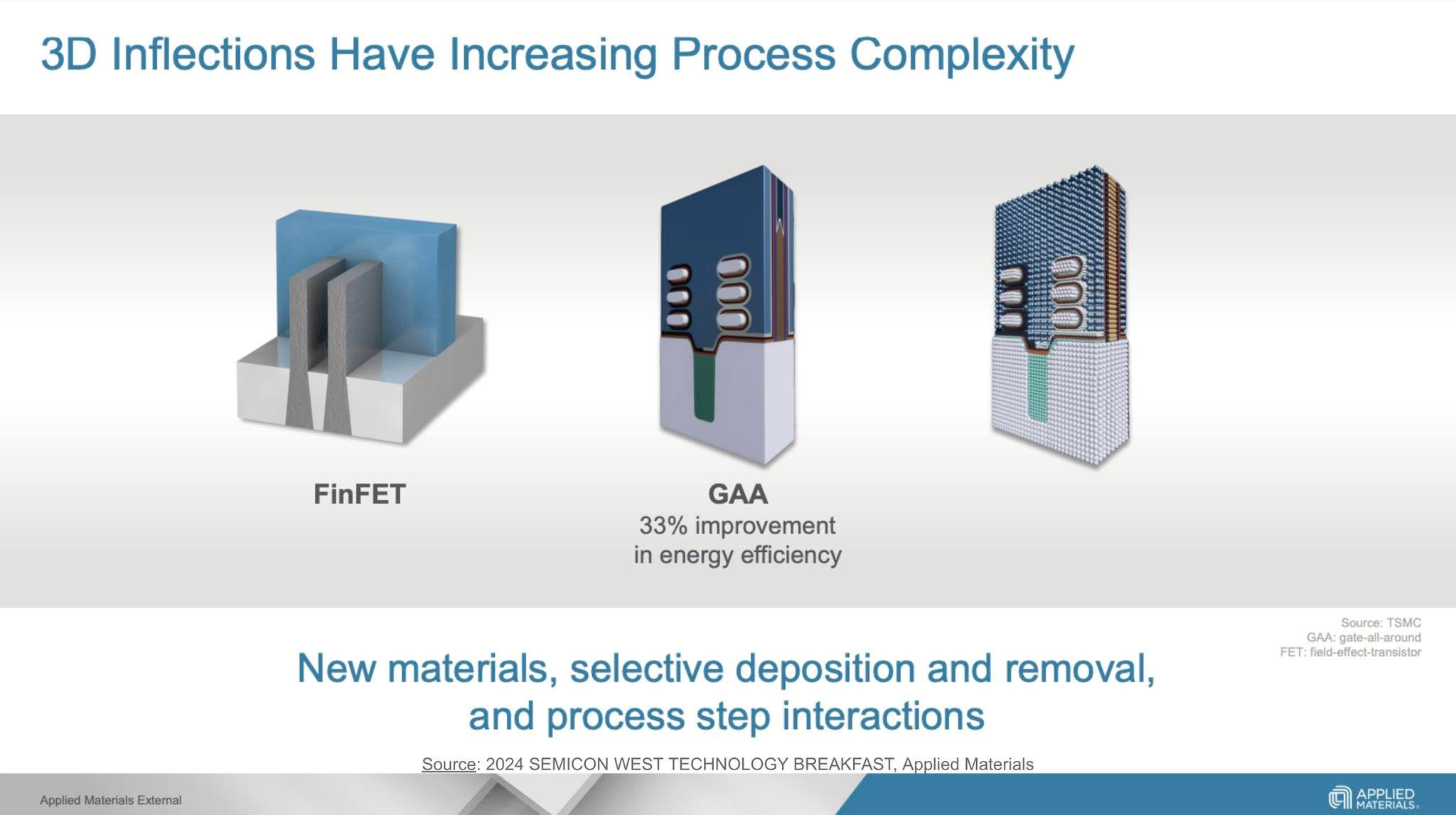
Unlocking the Future: TSMC’s Bold Strategy for the 2nm Revolution!

If validated, carbon nanotube CFETs could reshape the AI chip supply chain. Chinese AI labs — DeepSeek, Zhipu, Alibaba's Qwen team — are already shifting to domestic silicon, with Huawei's Ascend chips projected to reach 2030 targets via the Tau Scaling Law V2 paper. A carbon nanotube fab process would decouple AI chip performance from EUV access, potentially accelerating China's AI compute independence within 3-5 years.

The development also pressures TSMC and Samsung, who are investing $40B+ in 2nm EUV fabs. A disruptive non-silicon architecture could render those investments partially stranded if performance claims hold at scale.

What to watch

Watch for the peer-reviewed paper or independent replication. If a Chinese foundry (SMIC, Huawei) announces a pilot line within 12 months, the claim has legs. Also track TSMC's 2nm yield disclosures — if they remain below 60%, the CFET narrative strengthens.


Source: news.google.com


Sources cited in this article

  1. TrendForce
Source: gentic.news · · author= · citation.json

AI-assisted reporting. Generated by gentic.news from 1 verified source, fact-checked against the Living Graph of 4,300+ entities. Edited by Ala SMITH.

Following this story?

Get a weekly digest with AI predictions, trends, and analysis — free.

AI Analysis

The claim is technically plausible but historically fragile. Carbon nanotube transistors have been 'breakthrough of the year' in labs for a decade without commercial scale. The key missing piece is yield at wafer scale — a CFET cell is useless if defect density exceeds 1/cm². The 3x performance claim likely comes from TCAD simulations, not fabricated devices. China's motivation is clear: EUV denial creates a $50B+ incentive to find alternatives. But the gap between a lab demo and a foundry-ready process is typically 5-7 years. Compare to TSMC's 2nm timeline: risk production in 2025, volume in 2026. If this CFET claim is real, we'd expect SMIC to announce a pilot line within 12 months. Until then, treat as PR signaling for domestic AI chip investment.
This story is part of
Hugging Face Becomes the Neutral Ground Where Google and Anthropic's Agent Protocol War Converges
As Claude Code's MCP dominance threatens Google Cloud, Hugging Face's unique position as partner to both players creates an unexpected convergence zone
Compare side-by-side
TSMC vs Samsung
Enjoyed this article?
Share:

AI Toolslive

Five one-click lenses on this article. Cached for 24h.

Pick a tool above to generate an instant lens on this article.

Related Articles

From the lab

The framework underneath this story

Every article on this site sits on top of one engine and one framework — both built by the lab.

More in AI Research

View all