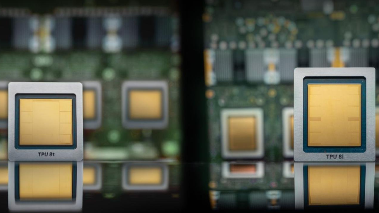
IBM demonstrated sub-1-nanometer chip technology at the IEDM conference, targeting production readiness within five years. The announcement positions IBM against TSMC's 2nm and Intel's 18A nodes in the race for extreme ultraviolet lithography.
Key facts
- IBM demonstrated sub-1-nm chip technology at IEDM.
- Targets production readiness within five years.
- TSMC plans 2nm production in late 2025.
- Intel's 18A node is slated for 2026.
- IBM's Albany Nanotech Center hosted the demo.
Key Takeaways
- IBM showed sub-1-nm chips at IEDM, targeting production in 5 years.
- It challenges TSMC and Intel in the race to shrink transistors for AI workloads.
The Sub-1-nm Breakthrough
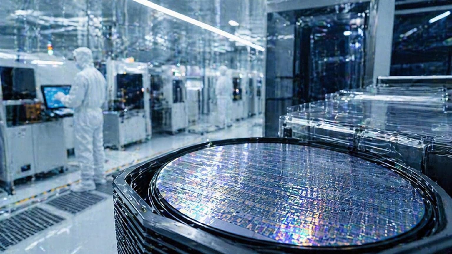
IBM demonstrated sub-1-nanometer chip technology at the IEDM conference, targeting production readiness within five years [According to EE Times](https://news.google.com/rss/articles/CBMiiAFBVV95cUxQVUhOTFFaQjhSSkFjM2EtLVpHT044WTJKX29WMUNWS21FeE96TnNmSjlpYnRTLXBUS0hZMGx3Z0daU05kM19jeHROaENxNVFvbDhtQ3ZDeXNoN0EyNTdjb0s5c3RlMloyaFdZTTZHdU5MbGQ1ZERPb2F6TlRHTURJS1I1c1k0NFcw?oc=5]. The technology uses a novel nanosheet transistor architecture that shrinks gate pitch beyond current extreme ultraviolet (EUV) lithography limits. IBM has not disclosed a specific process name for the sub-1-nm node, nor the exact transistor density per square millimeter.
Competitive Landscape
The announcement positions IBM against TSMC's 2nm and Intel's 18A nodes. TSMC plans 2nm production in late 2025, while Intel's 18A (equivalent to roughly 1.8nm) is slated for 2026. IBM's sub-1-nm target, if achieved, would skip multiple process generations. The company's Albany Nanotech Center in New York, where the demonstration took place, has been a key R&D site for advanced lithography since the 2014 $3 billion state investment.
The AI Angle
For AI training and inference, denser transistors directly translate to lower power per FLOP and higher throughput per die. IBM's sub-1-nm roadmap could enable chips with hundreds of billions of transistors, critical for models requiring massive parameter counts. However, IBM has not committed to manufacturing the node itself — it may license the design to foundries like Samsung.
Timeline and Risks
The five-year timeline to production is aggressive given that TSMC's 2nm, a much larger node, still faces yield challenges. EUV tools capable of sub-1-nm resolution — high-NA EUV from ASML — are not yet commercially deployed. IBM acknowledged the technology remains in early R&D phase and did not provide yield or power-performance numbers from the demonstration. The company has not specified which foundry partner, if any, would commercialize the process.
What to watch
Watch for IBM's next IEDM paper in 2027 with yield and power-performance data. Also monitor ASML's high-NA EUV tool deployment timeline — without those tools, sub-1-nm production is impossible. Any foundry partnership announcement would signal commercialization intent.
Source: news.google.com