China's DFSX SuperNode claims 2x the memory bandwidth of NVIDIA's GB200 NVL72, per Wccftech. The 14nm design skips microbumps for vertical compute-memory towers, but no benchmarks or ship dates are disclosed.
Key facts
- DFSX SuperNode claims 2x GB200 NVL72 memory bandwidth
- 14nm process with vertical compute-memory towers
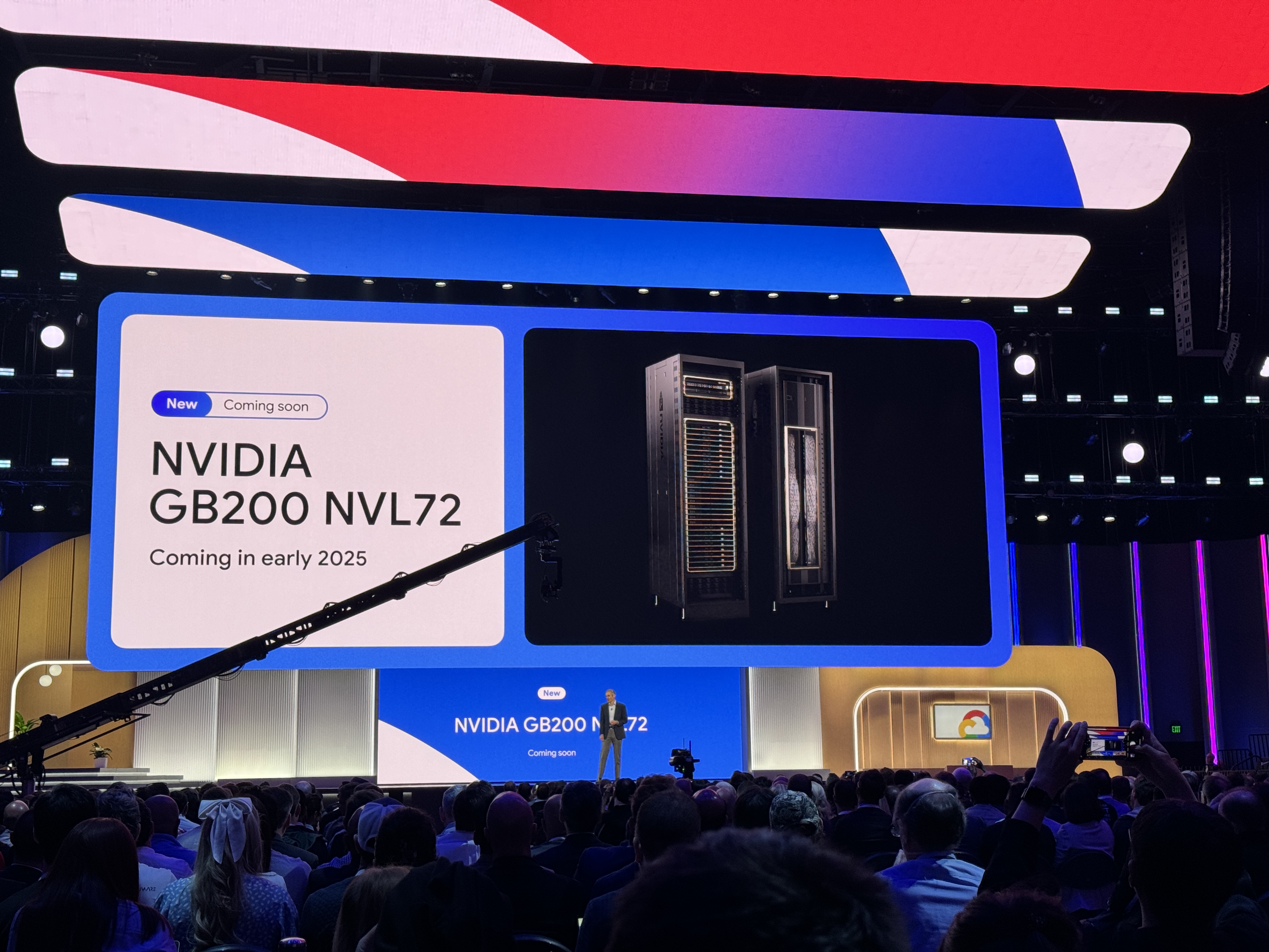
- GB200 NVL72: 72 Blackwell GPUs + 36 Grace CPUs
- No benchmark data or shipping timeline disclosed
- 14nm trails NVIDIA's 4nm-class Blackwell process
China's DFSX SuperNode claims to deliver 2x the memory bandwidth of NVIDIA's GB200 NVL72 system, according to a Wccftech report. The design reportedly uses a 14nm process, a far older node than the 4nm-class process behind NVIDIA's Blackwell, yet claims a memory-bandwidth advantage by stacking compute and memory vertically and eliminating microbumps—the tiny solder connections used in conventional 2.5D packaging.
The memory-bandwidth math
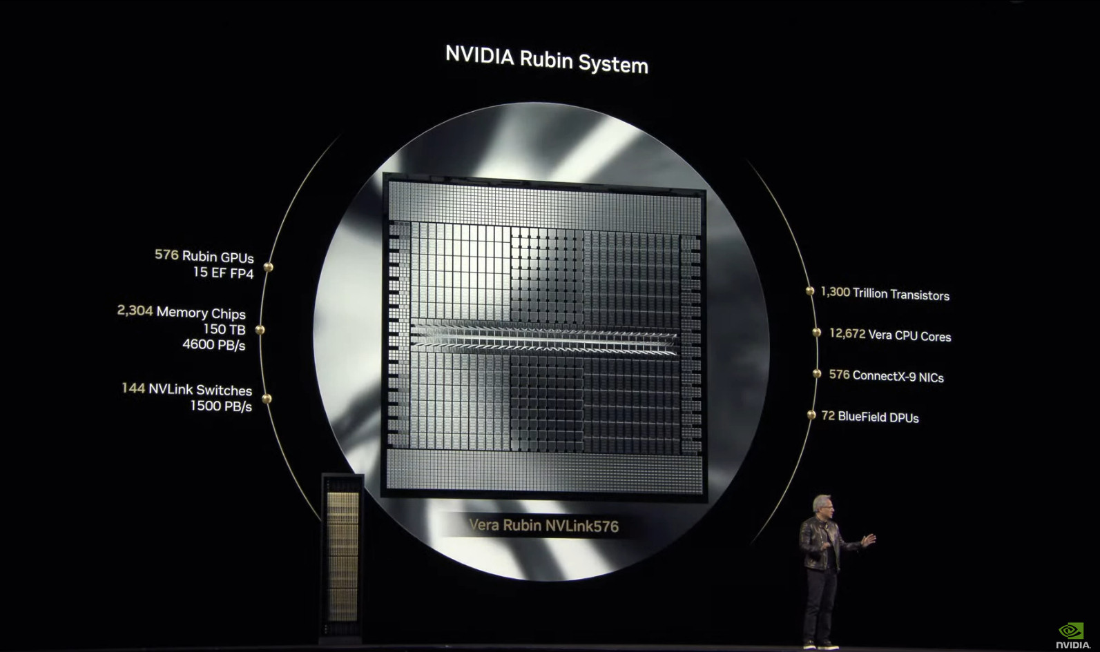
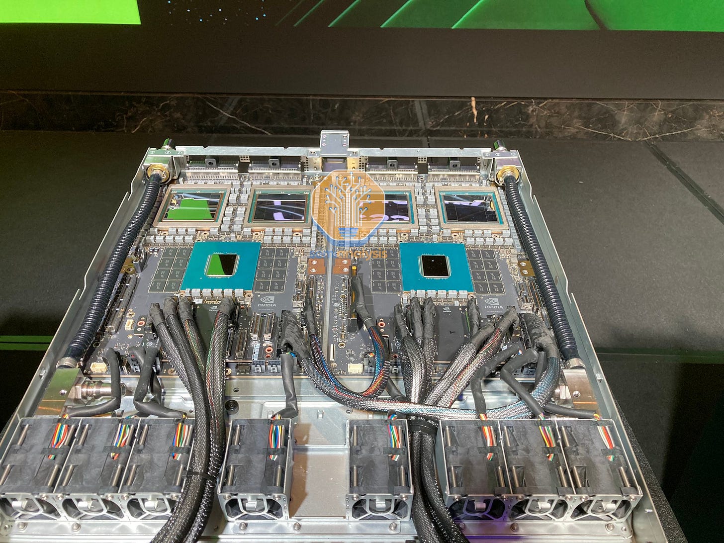
The GB200 NVL72 pairs 72 Blackwell GPUs with 36 Grace CPUs in a single rack, delivering roughly 30 TB/s of memory bandwidth per GPU via HBM3e. DFSX's SuperNode, if the claim holds, would push past 60 TB/s per compute unit—a figure that would rival or exceed NVIDIA's upcoming Vera Rubin platform, which is expected to move to HBM4. The vertical tower approach, similar in spirit to Samsung's X-Cube and Intel's Foveros Direct, trades the lateral interconnects of a reticle-sized interposer for a stacked die stack, reducing signal path length and potentially cutting power per bit moved. [Wccftech's report] provides no benchmark data, power figures, or shipping timeline for the DFSX SuperNode.
Skepticism warranted
The 14nm node is a red flag. TSMC's 7nm and 5nm classes have been in high-volume production since 2018 and 2020, respectively; a 14nm design would struggle to match Blackwell's transistor density and energy efficiency, even with a clever memory architecture. DFSX may be targeting a niche: inference workloads where memory bandwidth, not compute throughput, is the bottleneck. But without measured results, the 2x claim is marketing until proven otherwise. China's domestic chip push—SMIC's 7nm-class N+2 process, for example—has shown that advanced-node access remains constrained by US export controls, which may explain the reliance on a mature 14nm node. Reuters has previously reported that Chinese fabs are optimizing mature nodes for AI accelerators, but no DFSX product has appeared in any public benchmark suite.
What this means for the AI hardware race
If DFSX delivers even half the claimed bandwidth, it would represent a meaningful alternative for Chinese AI labs facing NVIDIA export restrictions. The vertical-tower approach could also inform Western designs: NVIDIA's own roadmap includes co-packaged optics and 3D stacking, but the company has not abandoned microbumps for its high-bandwidth memory interfaces. The real test is whether DFSX can scale beyond a single SuperNode—memory bandwidth per rack is one thing, but cluster-level interconnect and software ecosystem are what make GB200 NVL72 dominant. The report is silent on those fronts.
What to watch
Watch for DFSX to publish any benchmark results or a product launch date. If the SuperNode appears in MLPerf or a Chinese equivalent like AIBench within 12 months, the claim deserves scrutiny. Also track whether SMIC or another foundry ramps 14nm AI-specific processes, which would signal real production intent.
Source: news.google.com