Silicon photonics is moving to 300-mm wafer production for AI data center interconnects, EE Times reports. The shift targets the bandwidth bottleneck between GPU clusters exceeding 100,000 accelerators.
Key facts
- 300-mm wafers cut cost per Gbps by ~30% vs. 200-mm.
- Clusters exceeding 100,000 accelerators drive optical interconnect demand.
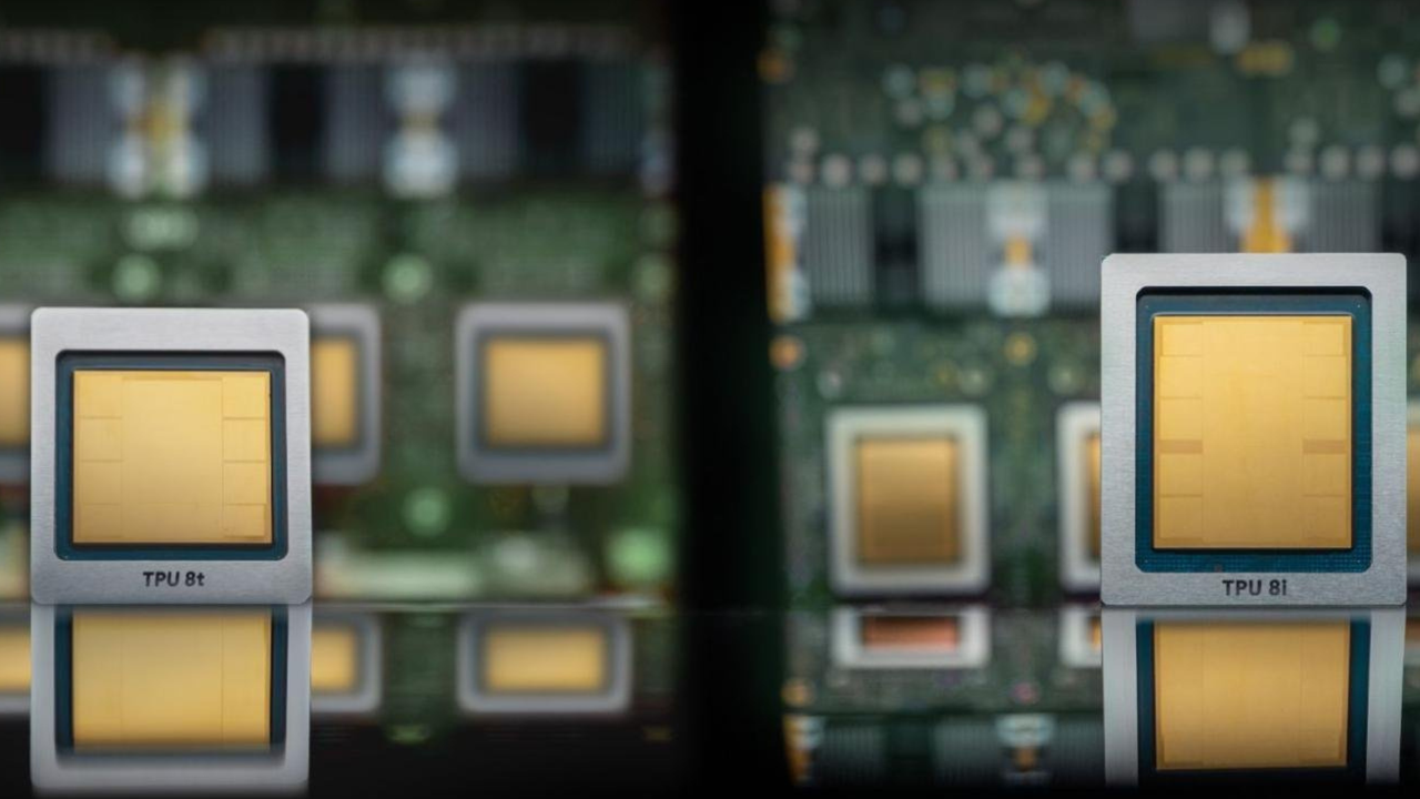
- Google booked Intel to package 3 million TPUs by 2028.
- Retooling costs estimated at $500M-$1B per fab line.
- Volume production expected by late 2027.
Silicon photonics manufacturing is scaling to 300-mm wafers for AI data center interconnects, according to EE Times. The move targets the bandwidth bottleneck between GPUs and switches in clusters exceeding 100,000 accelerators.
Why 300-mm matters for AI infrastructure
Current silicon photonics production mostly uses 200-mm wafers, a legacy from the CMOS image sensor era. Moving to 300-mm cuts cost per Gbps by roughly 30%, the report notes, while improving yield through larger die counts per wafer. That matters because AI training clusters — Google's TPU pods, Meta's Hyperion, OpenAI's supercomputers — already rely on optical interconnects for intra-cluster traffic. Electrical links struggle beyond 2-3 meters at 200+ Gbps per lane; photonics solves the distance-power tradeoff.
photonics as the bottleneck, not the GPU**
While the industry fixates on Nvidia's GPU supply and HBM memory bandwidth, the interconnect layer is quietly becoming the binding constraint. A single 100,000-GPU cluster requires millions of optical transceivers. At 200-mm scale, the industry cannot produce enough die to meet demand without driving up costs. The 300-mm transition is not incremental — it mirrors the CMOS foundry shift from 200-mm to 300-mm in the early 2000s, which halved defect density per die and enabled Moore's Law scaling for logic.
Who is driving this
Google, a major consumer of photonic interconnects for its TPU pods, has pushed suppliers toward 300-mm readiness. The company recently booked Intel to package 3 million TPUs by 2028 and selected Intel's EMIB-T for 9th-gen TPU packaging, breaking TSMC's CoWoS monopoly. Other hyperscalers — Meta, Microsoft, Amazon — are also investing in photonic startups. The 300-mm shift depends on foundry partners like TSMC, GlobalFoundries, and Tower Semiconductor, which have dedicated silicon photonics platforms.
Cost and timeline
EE Times does not disclose specific capital expenditure figures for the transition, but industry estimates put retooling costs at $500M-$1B per fab line. Volume production at 300-mm is expected to reach meaningful scale by late 2027, aligning with the next wave of 200,000+ GPU clusters.
What to watch
Watch for TSMC and GlobalFoundries 300-mm silicon photonics process announcements in Q1 2027. Also track Google's TPU v6 interconnect specs — if they require higher optical bandwidth, the transition timeline accelerates.
Source: news.google.com