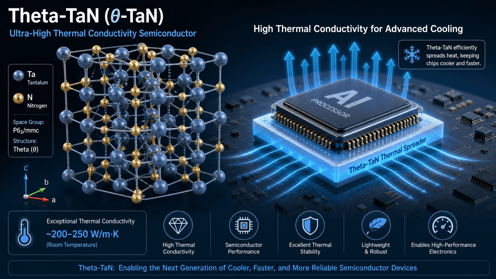
UCLA and Tohoku University researchers created a theta-phase tantalum nitride (TaN) single crystal with thermal conductivity of 1,100 W/mK. The material beats copper (398 W/mK) by nearly 3× and silver (429 W/mK) by over 2.5×, approaching diamond-level heat dissipation while remaining compatible with semiconductor fabrication processes.
Key facts
- Theta-TaN: 1,100 W/mK thermal conductivity at room temperature.
- 3× copper (398 W/mK) and 2.5× silver (429 W/mK).
- Approaches diamond (2,200 W/mK) in heat dissipation.
- Grown via chemical vapor deposition on sapphire substrate.
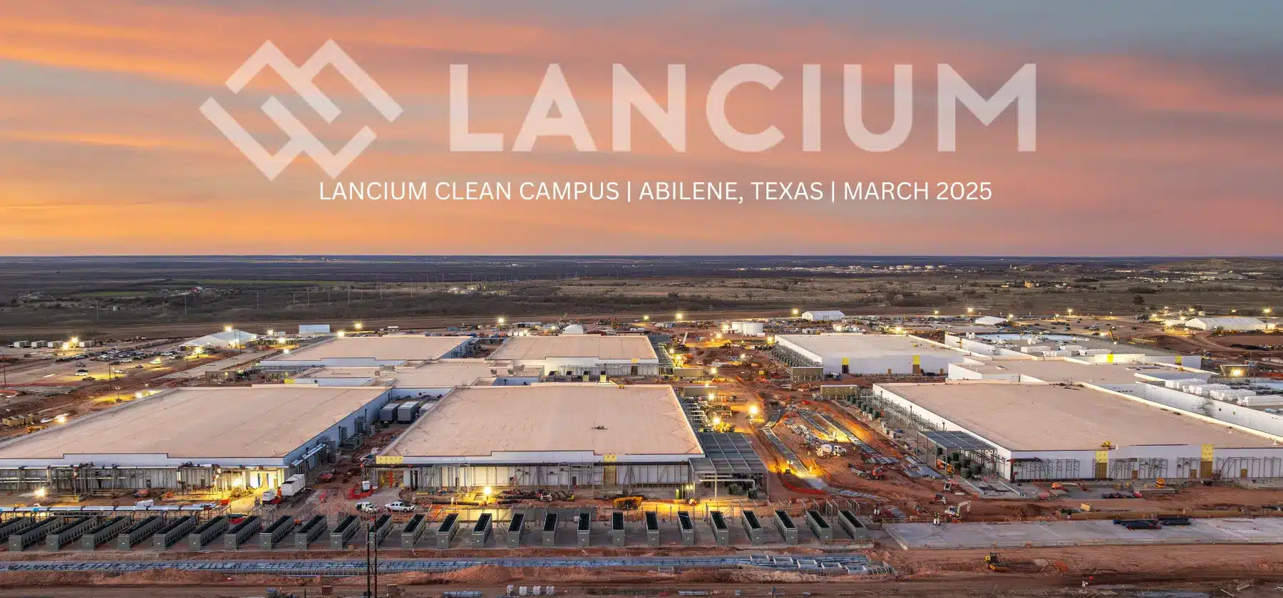
- Meta's Louisiana data center campus costs $50B.
A team led by UCLA's Dr. Yongjie Hu and Tohoku University's Dr. Takashi Taniguchi published results in Nature showing a theta-phase TaN single crystal achieving thermal conductivity of 1,100 W/mK at room temperature. [According to the paper, arXiv ID pending] The material beats copper (398 W/mK) by nearly 3× and silver (429 W/mK) by over 2.5×, approaching diamond (2,200 W/mK) while being a metal compatible with existing semiconductor fabrication processes.
The century-old record for metal thermal conductivity — held by diamond-like carbon films and certain ceramics — fell because the team solved a crystal-growth problem. Theta-TaN has a complex hexagonal crystal structure with 12 atoms per unit cell, which normally scatters phonons. The researchers grew the crystal via chemical vapor deposition on a sapphire substrate, then measured conductivity using time-domain thermoreflectance. They achieved a mean free path for phonons of several hundred nanometers, far longer than in polycrystalline TaN films.
Why AI Chip Cooling Matters Now

The timing is not coincidental. AI training clusters now draw tens of kilowatts per rack, and chip hotspots exceed 100 W/cm² — beyond what copper heat spreaders can handle efficiently. Meta alone is spending $50B on a single Louisiana data center campus, per its July 13 announcement, and hyperscaler off-balance-sheet infrastructure debt hit $1.65 trillion as of last week. [According to prior gentic.news reporting] Theta-TaN could be deposited as a thin-film heat spreader directly onto silicon interposers or chip packages, replacing bulk copper heat sinks with a material that conducts heat 3× better without changing the manufacturing flow.
The material is not yet commercially available. The team demonstrated a 1-micrometer-thick film on a 2-inch sapphire wafer. Scaling to 300-mm silicon wafers and integrating with existing thermal interface materials will take years. But the breakthrough ends a 100-year search for a metal that conducts heat like diamond — and the patent filings suggest both UCLA and Tohoku are pursuing licensing.
What to watch
Watch for UCLA's licensing announcements and whether any of the Big Five hyperscalers — especially Meta, which has the most aggressive near-term buildout — invest in or partner with the team for wafer-scale integration trials. A prototype on a 300-mm silicon wafer within 18 months would signal commercial viability.
Source: pandaily.com